
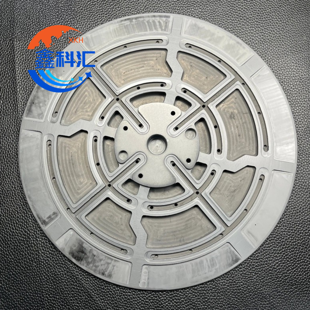
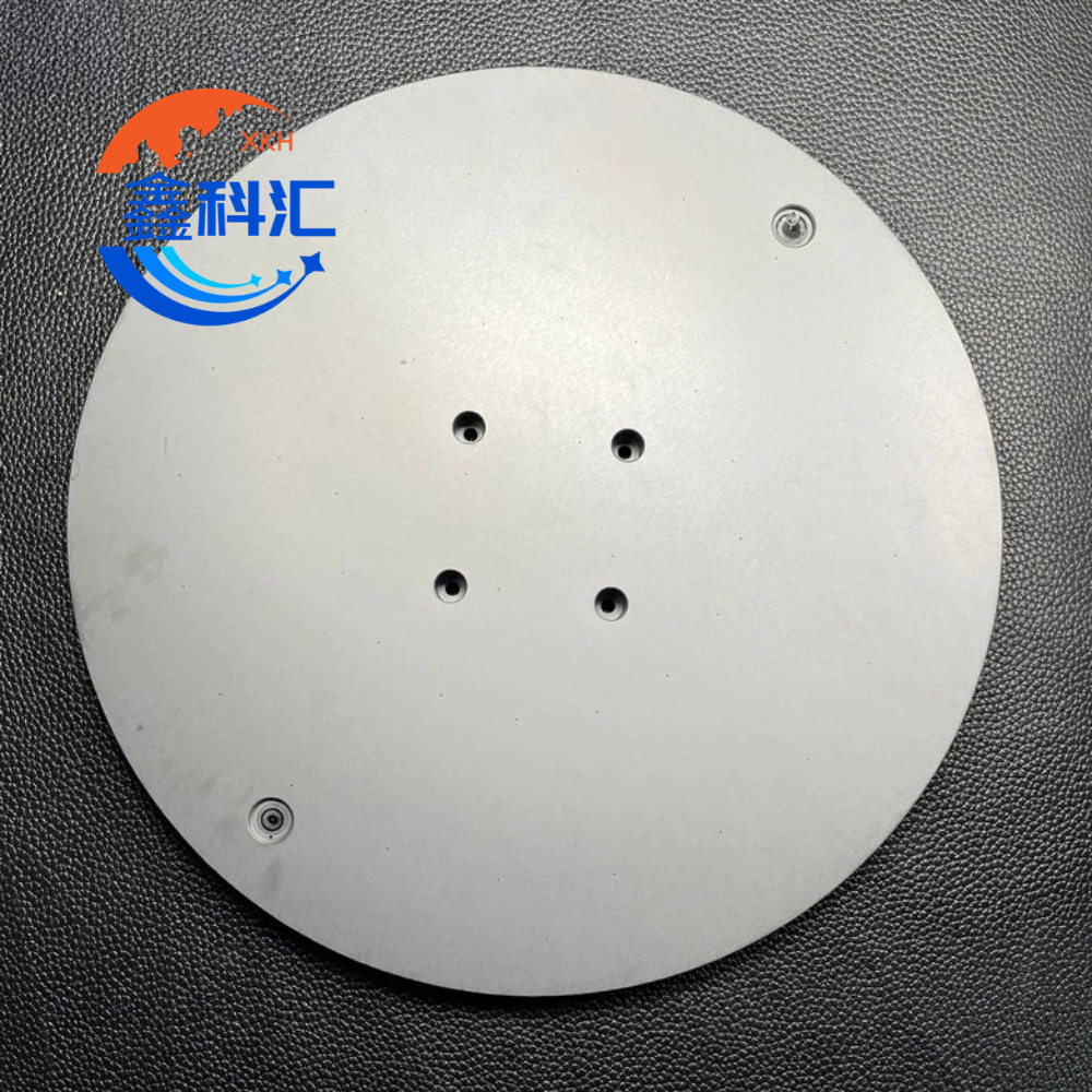
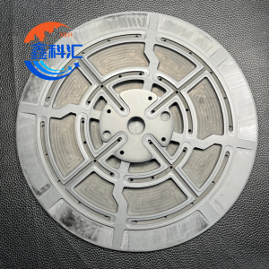
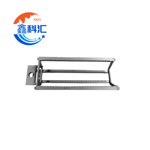
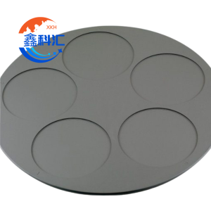
 The silicon carbide wafer tray is a high-performance precision ceramic carrier designed for semiconductor wafer processing, CVD/PECVD systems, vacuum furnaces, and high-temperature industrial environments.
Manufactured from high-purity CVD SiC or SSiC (sintered silicon carbide), this tray offers outstanding thermal stability, mechanical strength, and chemical resistance, ensuring stable wafer handling and consistent process performance in extreme conditions.
It is widely used in semiconductor manufacturing, LED epitaxy, sapphire wafer processing, advanced ceramics sintering, and vacuum thermal systems.
Основные характеристики
High Temperature Stability (Up to 1600°C+)
Maintains structural integrity and performance under continuous high-temperature operation without deformation.
Отличная теплопроводность
Ensures fast and uniform heat transfer, reducing temperature gradients and improving process yield.
Superior Thermal Shock Resistance
Withstands rapid heating and cooling cycles without cracking or warping.
Высокая механическая прочность
Reinforced structure provides excellent load-bearing capacity and long-term dimensional stability.
Chemical & Plasma Resistance
Highly resistant to acids, alkalis, corrosive gases, and plasma environments used in semiconductor processes.
Ultra-High Precision Machining
CNC grinding ensures tight tolerances, flatness, and smooth wafer contact surfaces for automated systems.
Structural Design
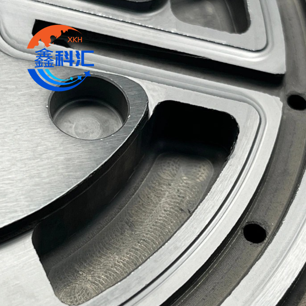
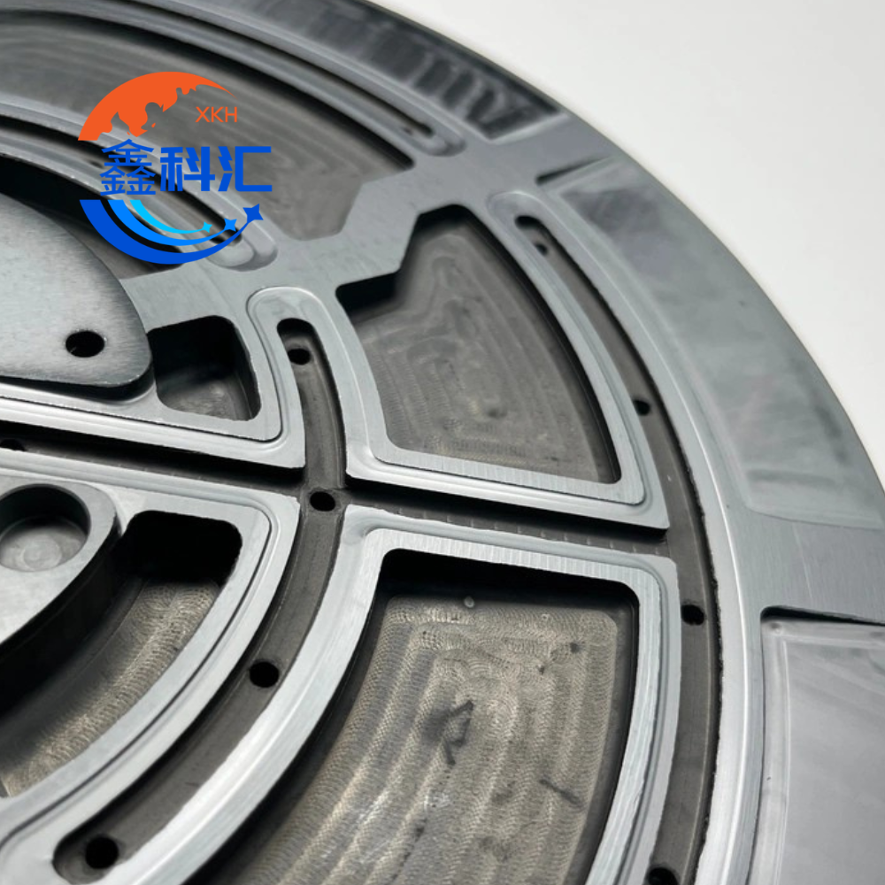
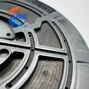
Multi-Zone Annular Slot Design
- Reduces weight
- Improves thermal uniformity
- Enhances heat dissipation
- Minimizes thermal stress concentration
This structure is optimized for high-temperature wafer processing and vacuum applications.
Radial Reinforcement Rib System
- Increases mechanical rigidity
- Prevents deformation under load
- Improves rotational stability
- Extends service life in cyclic thermal environments
Precision Machined Surface
- High flatness and consistency
- Smooth wafer contact interface
- Compatible with robotic automation systems
- Reduces particle generation risk
Central Mounting Interface
Precision-drilled center structure ensures:
- Stable shaft mounting
- Accurate alignment in furnace systems
- Compatibility with automated wafer handling equipment
Reinforced Outer Ring
- Enhances structural balance
- Improves vibration resistance
- Strengthens edge durability during operation
Варианты материалов
Карбид кремния CVD (CVD SiC)
- Сверхвысокая чистота
- Extremely low contamination
- Excellent surface quality
- Ideal for advanced semiconductor processes
Спеченный карбид кремния (SSiC)
- High strength and density
- Отличная износостойкость
- Stable in harsh environments
- Suitable for industrial high-temperature systems
Reaction-Bonded SiC (RBSiC)
- Экономически эффективное решение
- Хорошая устойчивость к тепловым ударам
- Suitable for mass industrial applications
Технические характеристики
| Артикул | Технические характеристики |
|---|---|
| Материал | CVD SiC / SSiC / RBSiC |
| Чистота | Up to 99.9% |
| Рабочая температура | ≤ 1600°C |
| Плотность | 2.3 – 3.9 g/cm³ |
| Устойчивость к тепловому удару | Превосходно |
| Отделка поверхности | Precision Ground / Polished |
| Форма | Custom (Round / Ring / Plate) |
| Размер | Доступно на заказ |
| Приложение | Semiconductor / CVD / Furnace |
Приложения
Полупроводниковая промышленность
- Wafer carrier for CVD / PECVD systems
- Diffusion, oxidation, annealing processes
- RTP and epitaxial growth systems
- Wafer transfer and handling trays
LED & Optoelectronics
- Sapphire wafer processing
- LED epitaxy carrier systems
- High-temperature substrate support
Vacuum & Thermal Furnaces
- High-temperature sintering trays
- Vacuum furnace carriers
- Thermal processing fixtures
Advanced Manufacturing
- Precision ceramic processing
- Automation equipment fixtures
- High-stability mechanical platforms
 Преимущества продукции
- Отличная устойчивость к высоким температурам
- Superior thermal conductivity
- Высокая стабильность размеров
- Длительный срок службы
- Low contamination risk
- Strong corrosion resistance
- Compatible with vacuum systems
- Fully customizable design
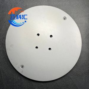 Customization Capability
We support full customization based on drawings or application requirements:
- Diameter / thickness customization
- Slot geometry optimization
- Precision mounting holes
- Surface polishing / lapping
- Ultra-flat wafer-grade machining
- High-purity material selection
- Complex structural design
OEM & ODM services available for semiconductor equipment manufacturers.
ЧАСТО ЗАДАВАЕМЫЕ ВОПРОСЫ
Q1: What is a silicon carbide wafer tray used for?
It is used to support and transport wafers during semiconductor processes such as CVD, PECVD, diffusion, oxidation, and high-temperature annealing.
Q2: Why use SiC instead of quartz or graphite?
SiC provides:
- Повышенная термостойкость
- Better mechanical strength
- Низкое тепловое расширение
- Более длительный срок службы
- Better chemical stability
Q3: Can the tray be customized?
Yes. We provide full customization including size, structure, thickness, and mounting design.
Q4: Is it suitable for rapid heating and cooling?
Yes. SiC has excellent thermal shock resistance, making it suitable for thermal cycling processes.
Отзывы
Отзывов пока нет.