

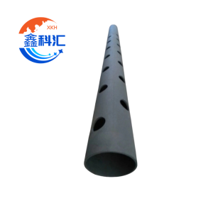
 The silicon carbide (SiC) horizontal process tube is designed for high-temperature LPCVD, CVD, diffusion, oxidation, and annealing applications in semiconductor, photovoltaic, and advanced materials manufacturing.
As the core reaction chamber component in horizontal thermal processing systems, the process tube directly affects temperature uniformity, contamination control, process stability, and overall equipment lifetime.
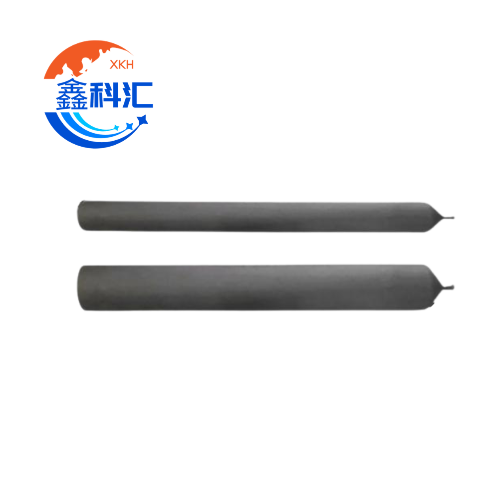
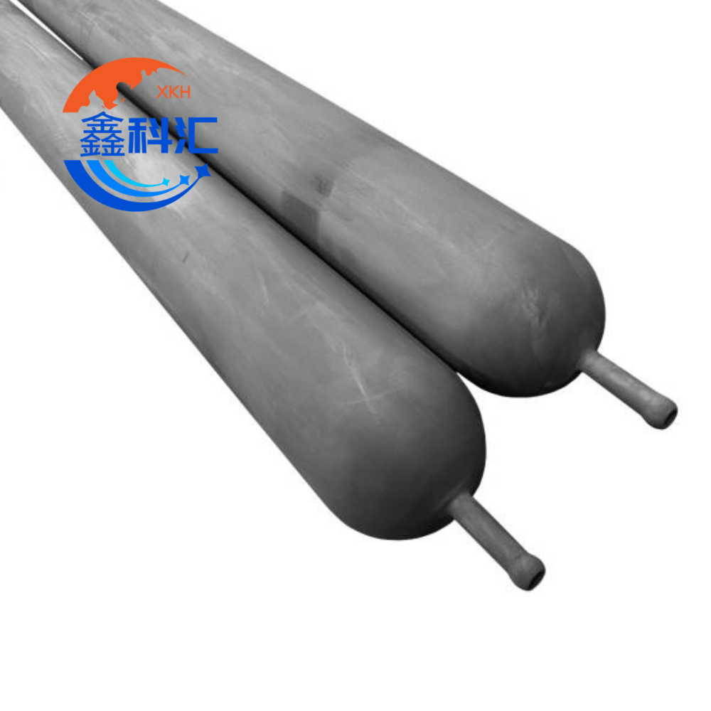
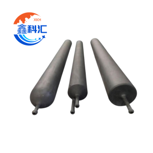
Our SiC horizontal process tubes are manufactured using advanced monolithic 3D printing technology combined with ultra-high-purity CVD silicon carbide coating. The seamless one-piece structure eliminates welding joints and assembly-related weak points, greatly improving mechanical reliability and leak resistance under continuous high-temperature operation.
Compared with conventional quartz process tubes, silicon carbide offers significantly higher thermal conductivity, better thermal shock resistance, superior corrosion resistance, and longer operational lifetime, especially in aggressive oxidizing and chlorine-containing process environments.
The product is optimized for semiconductor-grade clean processing environments requiring low particle generation, low metal contamination, and stable thermal performance up to 1250°C.
Key Features
 Monolithic One-Piece SiC Structure
The integrated 3D-printed silicon carbide body eliminates seams, brazing points, and potential leakage paths found in traditional assembled structures.
Benefits include:
- Higher structural stability
- Improved vacuum integrity
- Better dimensional consistency
- Reduced thermal stress concentration
Ultra-High Purity CVD SiC Coating
The dense CVD silicon carbide coating provides:
- Surface impurities below 5 ppm
- Excellent chemical inertness
- Reduced particle contamination
- Superior resistance to oxidation and chlorine-bearing gases
This makes the process tube suitable for advanced semiconductor thermal processing applications.
Excellent Thermal Conductivity
Silicon carbide provides much higher thermal conductivity than quartz or alumina, helping achieve:
- Faster thermal response
- Improved axial and radial temperature uniformity
- Stable wafer processing conditions
Outstanding Thermal Shock Resistance
The tube can withstand repeated rapid heating and cooling cycles without cracking, deformation, or coating spallation.
Long Service Life
Compared with quartz process tubes, SiC tubes offer:
- Longer replacement intervals
- Lower maintenance frequency
- Reduced chamber downtime
- Improved total cost of ownership (TCO)
Typical Applications
 Semiconductor Manufacturing
Suitable for:
- LPCVD systems
- CVD deposition equipment
- Oxidation furnaces
- Diffusion furnaces
- Annealing systems
- Wafer thermal treatment processes
Photovoltaic Industry
Used in:
- Solar cell diffusion processing
- Surface passivation
- Thin-film deposition
- High-temperature wafer treatment
Advanced Materials Processing
Applicable to:
- Carbonization processes
- Nitridation treatment
- Functional thin-film formation
- Surface activation and modification
Process Compatibility
Compatible Process Atmospheres
- Oxygen (O₂)
- Nitrogen (N₂)
- High-purity inert gases
- Controlled chlorine-containing gases
- Oxidizing atmospheres
Typical Process Window
| Parameter | Specification |
|---|---|
| Maximum Continuous Operating Temperature | 1250°C |
| Pressure Range | LPCVD Vacuum to Near Atmospheric |
| Thermal Shock Resistance | Excellent |
| Leak Tightness | ≤ 1×10⁻⁹ Pa·m³/s |
| Surface Roughness | Ra ≤ 0.8–1.6 µm |
| Coating Purity | < 5 ppm |
| Substrate Impurity | < 300 ppm |
Technical Specifications
| Item | Specification |
| Product Name | Silicon Carbide Horizontal Process Tube |
| Material | High Purity Silicon Carbide |
| Coating | CVD SiC Coating |
| Manufacturing Process | Monolithic 3D Printing |
| Maximum Operating Temperature | ≤ 1250°C |
| Thermal Conductivity | High |
| Thermal Shock Resistance | Excellent |
| Corrosion Resistance | Excellent |
| Surface Roughness | Ra ≤ 0.8–1.6 µm |
| Coating Impurities | < 5 ppm |
| Leak Tightness | ≤ 1×10⁻⁹ Pa·m³/s |
| Typical Applications | LPCVD / CVD / Diffusion / Oxidation |
Advantages Over Traditional Process Tubes
| Property | SiC Process Tube | Quartz Tube | Alumina Tube |
| Thermal Conductivity | High | Low | Low |
| Thermal Shock Resistance | Excellent | Weak | Moderate |
| Corrosion Resistance | Excellent | Moderate | Good |
| Particle Control | Excellent | Moderate | Moderate |
| Service Life | Long | Short | Medium |
| High-Temperature Stability | Excellent | Moderate | Good |
Customization Options
Custom specifications are available according to customer equipment requirements, including:
- Tube diameter and length
- Wall thickness optimization
- Flange and interface structures
- Functional gas ports
- Inner/outer coating configurations
- Surface polishing grades
- Cleanliness standards
FAQ
Q1: Why choose silicon carbide instead of quartz process tubes?
Silicon carbide provides higher thermal conductivity, lower contamination, better thermal shock resistance, and significantly longer service life than quartz, especially in high-temperature semiconductor processes.
Q2: What processes are compatible with this tube?
The tube is suitable for LPCVD, CVD, diffusion, oxidation, annealing, passivation, and other high-temperature thermal processing applications.
Q3: Can the tube operate in chlorine-containing atmospheres?
Yes. The CVD SiC coating offers excellent resistance to controlled chlorine-bearing process environments.
Reviews
There are no reviews yet.