シンケホイ

半導体用セラミックス:現代のエレクトロニクスを支える先端材料

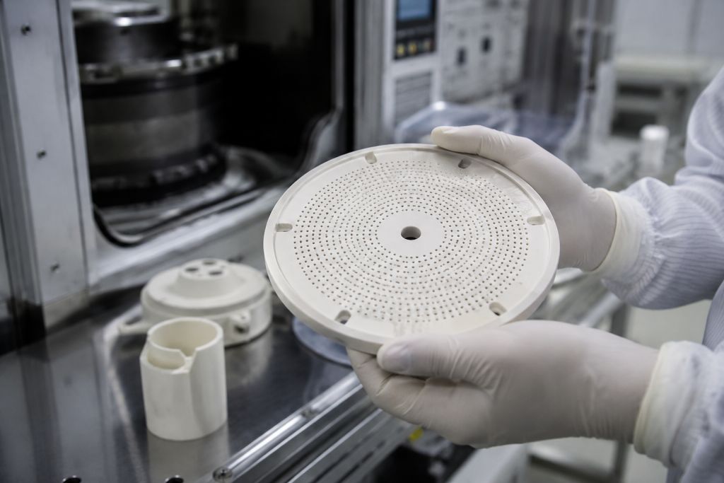
As semiconductor devices continue to become smaller, faster, and more powerful, the materials used in semiconductor manufacturing equipment must meet increasingly demanding performance requirements. Traditional metals and polymers often struggle to withstand extreme temperatures, corrosive chemicals, plasma environments, and ultra-clean processing conditions. This is where semiconductor ceramics play a critical role. Advanced ceramic materials combine exceptional thermal stability, electrical insulation, mechanical strength, wear resistance, and chemical durability, making them indispensable in semiconductor fabrication, power electronics, and advanced packaging technologies. Today, semiconductor ceramics are widely used in wafer processing equipment, plasma chambers, vacuum systems, electronic substrates, sensors, and next-generation power devices. What Are Semiconductor Ceramics? Semiconductor ceramics belong to a broader […]

半導体用セラミックス:現代のエレクトロニクスを支える先端材料 続きを読む »

炭化ケイ素セラミックが優れた耐摩耗性と耐食性を提供する理由

Advanced ceramic materials have become increasingly important in industries that demand exceptional durability, chemical stability, and long service life. Among these materials, silicon carbide (SiC) ceramics have gained widespread recognition for their outstanding wear resistance and corrosion resistance. As a result, silicon carbide components are widely used in semiconductor manufacturing, chemical processing, energy production, mining, aerospace, and mechanical engineering. The superior performance of silicon carbide ceramics is not merely the result of high hardness. Instead, it arises from a unique combination of crystal structure, strong atomic bonding, low porosity, and excellent chemical inertness. Understanding these characteristics helps explain why silicon carbide remains one of the most reliable engineering materials in

炭化ケイ素セラミックが優れた耐摩耗性と耐食性を提供する理由 続きを読む »

半導体セラミック部品製造プロセス:原料粉末から精密部品まで

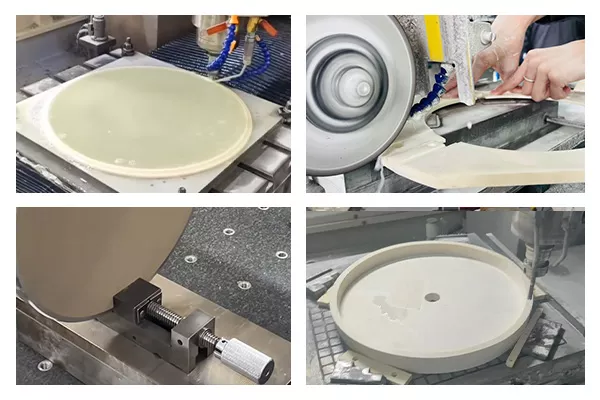
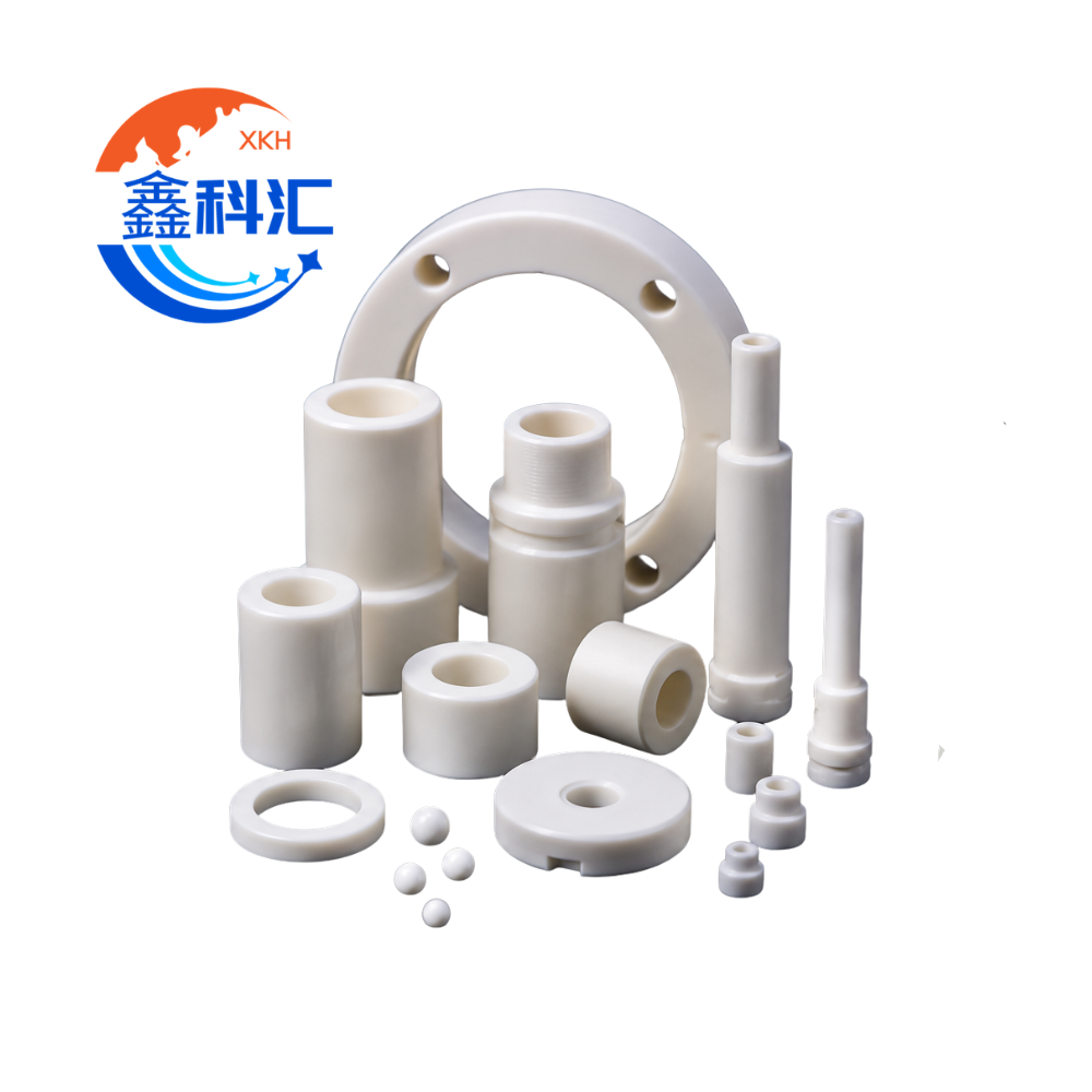
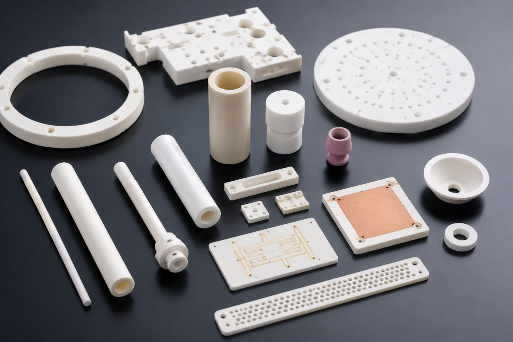
Modern semiconductor manufacturing relies heavily on advanced equipment such as etching systems, lithography machines, ion implantation tools, and deposition equipment. Inside these systems, numerous ceramic components play critical roles in ensuring process stability, precision, and reliability. Thanks to their exceptional high-temperature resistance, corrosion resistance, mechanical strength, dimensional stability, and electrical properties, advanced ceramic components are widely used throughout semiconductor fabrication processes. Many of these components come into direct contact with wafers and are responsible for precise temperature control, plasma resistance, vacuum handling, and contamination reduction. Common semiconductor ceramic materials include: Typical semiconductor ceramic components include: The manufacturing of semiconductor ceramic parts involves a series of highly controlled processes, including powder

半導体セラミック部品製造プロセス:原料粉末から精密部品まで 続きを読む »

精密工業用高純度ジルコニア部品

High purity zirconia parts are widely used in industries that demand exceptional wear resistance, corrosion resistance, dimensional stability, and mechanical strength. Compared with traditional metal materials and standard industrial ceramics, zirconia ceramics offer a unique combination of toughness and precision, making them suitable for advanced industrial systems. Today, high purity zirconia components are commonly found in semiconductor manufacturing, precision machinery, medical devices, chemical processing, fluid control systems, and high-speed bearing applications. What Are High Purity Zirconia Parts? High purity zirconia parts are precision ceramic components manufactured from zirconium dioxide (ZrO₂) with controlled purity and microstructure. These ceramics are engineered to provide superior mechanical and thermal performance in demanding environments. Depending

精密工業用高純度ジルコニア部品 続きを読む »

静電チャック vs 真空チャック:半導体製造におけるウェーハ保持技術はどちらが優れているか?

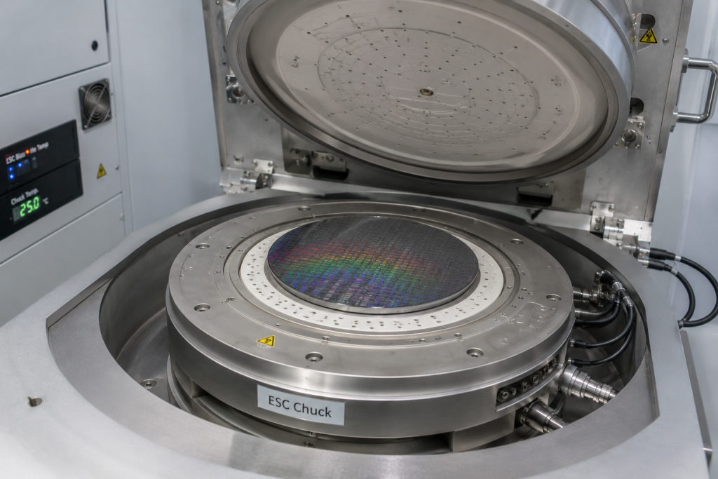
In semiconductor manufacturing, wafer positioning and fixation are fundamental requirements for achieving process precision and yield stability. During etching, deposition, lithography, inspection, and plasma processing, silicon wafers must remain securely held while maintaining minimal contamination and excellent thermal uniformity. As device structures continue shrinking and wafer sizes continue increasing, traditional holding methods face growing challenges. Two of the most widely used wafer fixation technologies today are Electrostatic Chucks (ESCs) and Vacuum Chucks. Although both systems serve the same general purpose—holding wafers in place—their working principles, operating environments, and performance characteristics differ significantly. Understanding these differences is essential for equipment designers, process engineers, and semiconductor manufacturers. Why Wafer Holding Technology Matters

静電チャック vs 真空チャック:半導体製造におけるウェーハ保持技術はどちらが優れているか? 続きを読む »

炭化ケイ素トレイが従来のウェハーキャリアに取って代わる理由

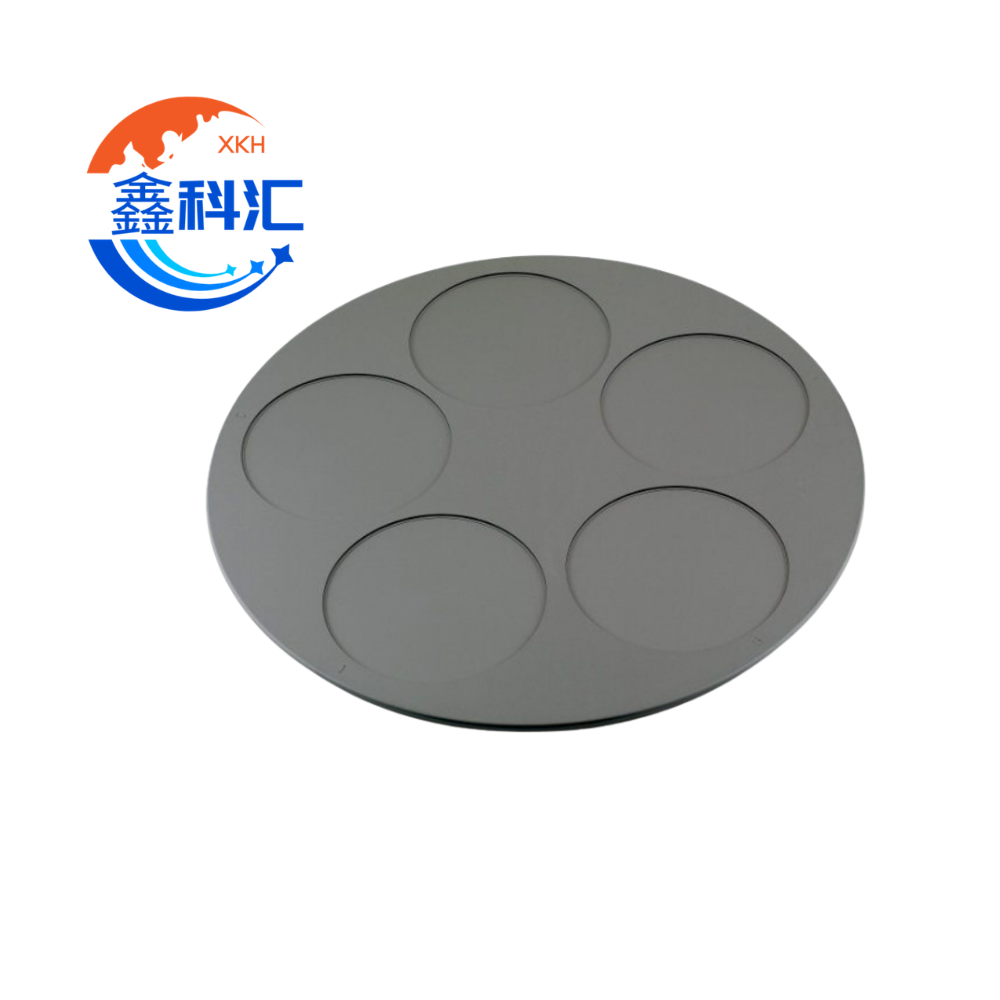
As semiconductor manufacturing continues moving toward larger wafer sizes, higher process temperatures, and stricter contamination standards, conventional wafer carrier materials are increasingly reaching their performance limits. Components that once met process requirements are now facing challenges involving thermal deformation, particle generation, and shorter service life. Among advanced ceramic materials, silicon carbide (SiC) trays have emerged as one of the most promising alternatives to traditional wafer carriers. Thanks to their superior thermal, mechanical, and chemical properties, SiC trays are increasingly being adopted in semiconductor processing equipment. But what is driving this shift? Why are silicon carbide trays gradually replacing conventional wafer carriers in high-end semiconductor manufacturing? This article explores the material

炭化ケイ素トレイが従来のウェハーキャリアに取って代わる理由 続きを読む »

セラミックヒートシンクとセラミックヒートスプレッダ:主な違いと技術的役割

In high-power electronics, semiconductor packaging, LED systems, and RF devices, thermal management is one of the most critical factors affecting performance and reliability. As power density continues to increase, two terms are frequently used: Ceramic Heatsink and Ceramic Heat Spreader. Although they sound similar, they serve very different roles in a thermal system. In simple terms, one is designed to spread heat, while the other is designed to remove heat from the system. 1. What is a Ceramic Heat Spreader? A ceramic heat spreader is not a final cooling device. Instead, it is an internal thermal management layer designed to redistribute concentrated heat. In electronic devices, heat is typically generated

セラミックヒートシンクとセラミックヒートスプレッダ:主な違いと技術的役割 続きを読む »

リソグラフィーからウェハー製造まで:炭化ケイ素セラミックスはいかにして10億ドル規模の半導体市場を動かしているのか?

When people think about the semiconductor industry, they usually focus on chips, wafers, or advanced process nodes. However, behind every semiconductor breakthrough lies a less visible but equally critical foundation: advanced materials. As semiconductor manufacturing continues to pursue higher precision, smaller geometries, and faster production speeds, equipment performance requirements are becoming increasingly demanding. This shift is creating new opportunities for advanced engineering materials—especially Silicon Carbide (SiC) ceramics. From lithography machines to wafer processing systems, silicon carbide ceramics are rapidly becoming key components in modern semiconductor equipment. Once considered a niche material, SiC ceramics are now helping build what many industry experts see as a future multi-billion-dollar market. The Hidden Material

リソグラフィーからウェハー製造まで:炭化ケイ素セラミックスはいかにして10億ドル規模の半導体市場を動かしているのか? 続きを読む »

なぜアドバンスト・セラミックスはエレクトロニクスで重要なのか?特性、用途、利点

The electronics industry is evolving toward higher power density, smaller device sizes, and more demanding operating environments. From semiconductor fabrication to power electronics and precision sensors, materials are expected to deliver stability under heat, prevent electrical interference, and maintain dimensional accuracy over long service periods. This is where advanced ceramics play a critical role. Materials such as alumina, zirconia, silicon carbide, and aluminum nitride have become essential in modern electronic systems due to their unique combination of electrical, thermal, and mechanical properties. What Are Advanced Ceramics? Advanced ceramics (also called technical ceramics or engineering ceramics) are high-performance inorganic materials engineered for demanding industrial applications. Unlike traditional ceramics used in pottery

なぜアドバンスト・セラミックスはエレクトロニクスで重要なのか?特性、用途、利点 続きを読む »

ジルコニアとアルミナ:どちらのセラミック材料が用途に適合するか?

Selecting the right technical ceramic material is critical for industrial applications where performance, durability, and cost directly affect productivity and long-term reliability. Among advanced engineering ceramics, Zirconia (ZrO₂) and Alumina (Al₂O₃) are two of the most widely used materials. Both materials offer exceptional hardness, wear resistance, and chemical stability. However, they differ significantly in toughness, strength, thermal properties, and application suitability. So which ceramic material is the better choice for your application? The answer depends on your operating environment and performance priorities. This article compares zirconia and alumina across key characteristics to help engineers, manufacturers, and purchasing teams make informed decisions. What Is Alumina Ceramic? Alumina ceramic, also known as

ジルコニアとアルミナ:どちらのセラミック材料が用途に適合するか? 続きを読む »

炭化ケイ素ウェハー・ボートと石英ウェハー・ボート:どちらが優れているか?

In semiconductor manufacturing, wafer handling components directly affect process stability, yield, and long-term operating cost. Among them, wafer boats play a critical role in transporting and supporting wafers during high-temperature diffusion, oxidation, epitaxy, and coating processes. Two of the most commonly used materials are Silicon Carbide (SiC) wafer boats and Quartz wafer boats. While both are widely used in semiconductor and precision manufacturing environments, they differ significantly in thermal performance, durability, contamination control, and lifecycle cost. So which one is better? The answer depends on your process requirements. This article compares SiC and quartz wafer boats across key performance factors to help manufacturers make a better choice. What Is a

炭化ケイ素ウェハー・ボートと石英ウェハー・ボート:どちらが優れているか? 続きを読む »

半導体装置用複雑構造セラミック部品の製造上の課題

In advanced semiconductor manufacturing, key process modules such as plasma etching, chemical vapor deposition (CVD), and ion implantation operate under extreme environments involving high-energy plasma, corrosive gases, high voltage bias, and rapid thermal cycling. These conditions impose stringent requirements on structural materials in terms of dielectric stability, corrosion resistance, thermal compatibility, and long-term dimensional reliability. Advanced engineering ceramics—such as alumina (Al₂O₃), aluminum nitride (AlN), silicon carbide (SiC), and silicon nitride (Si₃N₄)—have become indispensable due to their excellent combination of thermal, electrical, and chemical stability. However, the ongoing evolution of semiconductor equipment toward miniaturization and functional integration has driven ceramic components from simple geometries to highly complex architectures, including micro-channel networks,

半導体装置用複雑構造セラミック部品の製造上の課題 続きを読む »