テクニカル・インサイト

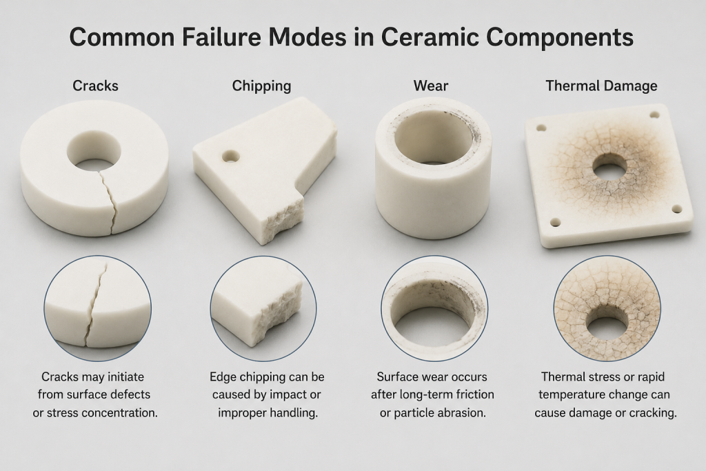
Ceramic Components Failure Analysis: Cracks, Chipping, Wear and Thermal Damage

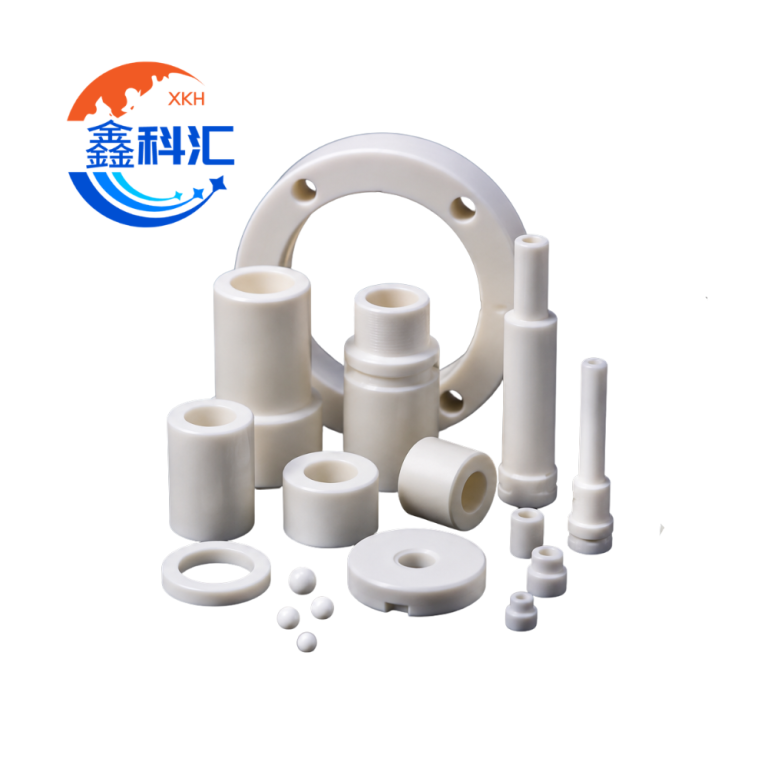
Advanced ceramic components are widely used in semiconductor equipment, vacuum systems, precision machinery, electrical insulation, chemical processing and high-temperature applications. Materials such as alumina, zirconia, aluminum nitride, silicon carbide and silicon nitride provide excellent hardness, wear resistance, corrosion resistance, electrical insulation and dimensional stability. Despite these advantages, ceramic components can still fail. Unlike most metals, technical ceramics usually undergo very little plastic deformation before fracture. A component may appear normal during operation and then crack or break suddenly. Small defects introduced during forming, sintering, machining, transportation or installation can gradually develop into serious failures under mechanical loading, temperature cycling, chemical exposure or repeated contact. Ceramic failure analysis should therefore go […]

Ceramic Components Failure Analysis: Cracks, Chipping, Wear and Thermal Damage 続きを読む »
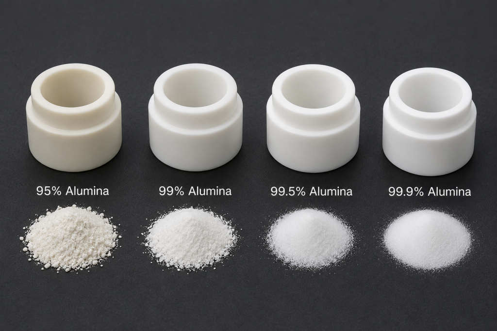
Alumina Ceramic Purity Levels Explained: 95%, 99%, 99.5% and 99.9% Compared

Alumina ceramic, also known as aluminum oxide ceramic or Al₂O₃ ceramic, is one of the most widely used technical ceramic materials. It offers a practical combination of electrical insulation, mechanical strength, hardness, wear resistance, thermal stability and corrosion resistance. However, not all alumina ceramics are the same. Commercial alumina materials are commonly identified by their nominal alumina content, such as: The remaining percentage normally consists of sintering additives, glassy phases and trace impurities used to control densification, grain growth, machinability and manufacturing cost. In general, increasing alumina purity can improve chemical stability, electrical insulation, high-temperature performance and resistance to plasma or process contamination. However, a higher percentage does not automatically

Alumina Ceramic Purity Levels Explained: 95%, 99%, 99.5% and 99.9% Compared 続きを読む »

Structural Ceramics for Semiconductor Manufacturing: Key Materials and Equipment Applications

Semiconductor manufacturing requires materials that can operate reliably under high temperature, plasma exposure, chemical corrosion, vacuum conditions and strict cleanliness requirements. In many process tools, metal and plastic components cannot meet these demanding conditions. This is why structural ceramics are widely used in semiconductor equipment. Structural ceramics are advanced ceramic materials designed to provide mechanical strength, dimensional stability, wear resistance, insulation and chemical resistance. In semiconductor manufacturing, they are used not only as supporting parts, but also as precision components that directly influence wafer handling, process stability and contamination control. What Are Structural Ceramics? Structural ceramics are ceramic materials used for load-bearing, positioning, supporting, insulating and protective functions. Unlike traditional

Structural Ceramics for Semiconductor Manufacturing: Key Materials and Equipment Applications 続きを読む »

Semiconductor Wafer Boat Materials: SiC, Quartz and Alumina Compared

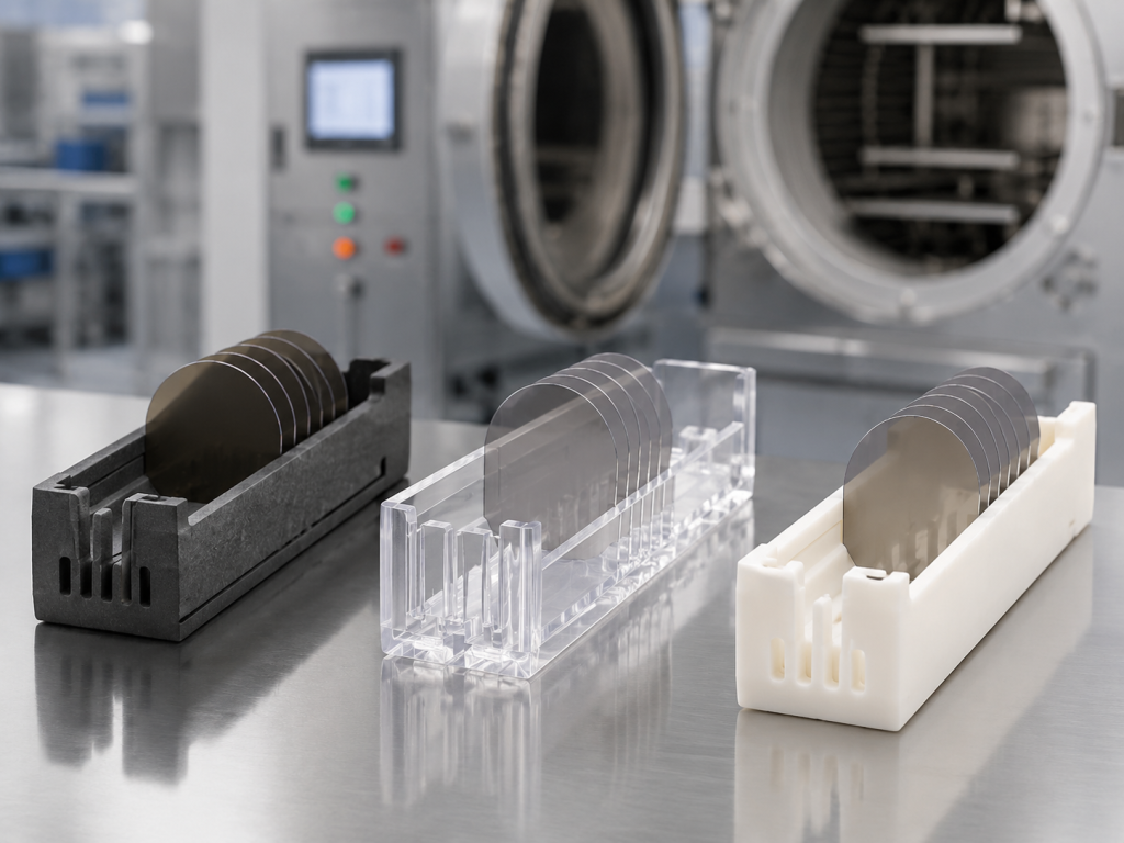
In semiconductor manufacturing, wafer boats are used to hold and support wafers during high-temperature processes such as diffusion, oxidation, annealing and LPCVD. Although the structure of a wafer boat may look simple, the material choice is very important. Different materials can affect thermal stability, contamination control, mechanical strength, service life and overall process reliability. Among the most commonly used wafer boat materials, silicon carbide, quartz and alumina ceramic are three important options. Each material has its own advantages and limitations. Choosing the right wafer boat material depends on the process temperature, wafer type, furnace environment, cleanliness requirements and cost considerations. This article compares SiC, quartz and alumina wafer boats to

Semiconductor Wafer Boat Materials: SiC, Quartz and Alumina Compared 続きを読む »

半導体ウェーハボートとは? 材質、構造、および用途

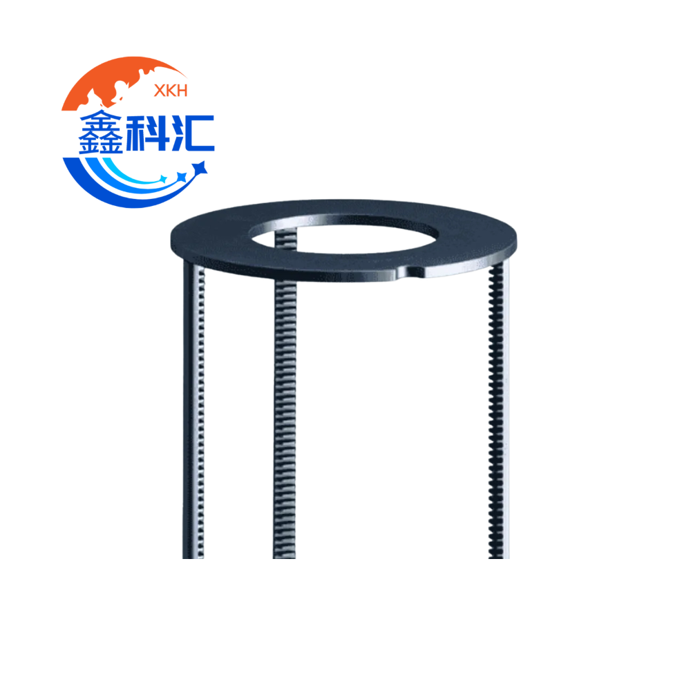
In semiconductor manufacturing, wafers must be processed, transported, heated and cooled under highly controlled conditions. During high-temperature processes such as diffusion, oxidation, annealing and LPCVD, wafers cannot simply be placed directly inside a furnace. They need a stable, clean and precisely designed carrier to hold them in position. This carrier is commonly known as a semiconductor wafer boat. A wafer boat may look like a simple supporting fixture, but it plays an important role in process stability, wafer cleanliness and production yield. The choice of wafer boat material, structure and dimensional accuracy can directly affect thermal uniformity, particle control, wafer spacing and long-term equipment reliability. What Is a Semiconductor Wafer

半導体ウェーハボートとは? 材質、構造、および用途 続きを読む »

Overcoming the Challenges of Manufacturing Complex Semiconductor Ceramic Components

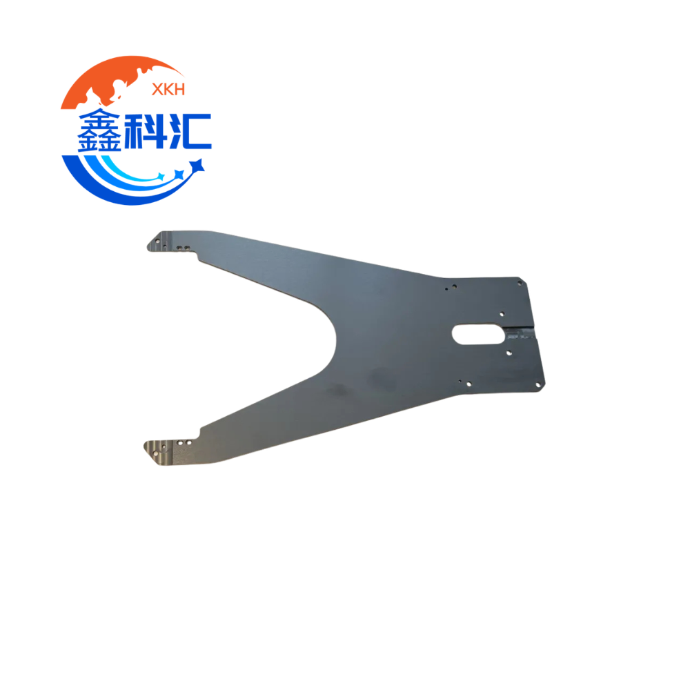
Advanced ceramics have become indispensable materials in modern semiconductor equipment. Components used in plasma etching, chemical vapor deposition (CVD), physical vapor deposition (PVD), ion implantation, and wafer handling systems must operate reliably under extreme conditions, including high-energy plasma exposure, corrosive process gases, elevated temperatures, thermal cycling, and high-voltage electrical fields. Materials such as alumina (Al₂O₃), aluminum nitride (AlN), silicon carbide (SiC), and silicon nitride (Si₃N₄) offer exceptional hardness, electrical insulation, thermal stability, and plasma resistance. However, these same properties also make them among the most difficult engineering materials to manufacture. As semiconductor devices continue to evolve toward higher integration and smaller process nodes, ceramic components are becoming increasingly complex. Traditional

Overcoming the Challenges of Manufacturing Complex Semiconductor Ceramic Components 続きを読む »

多孔質炭化ケイ素(SiC)セラミック担体:低温焼結技術と性能に関する研究

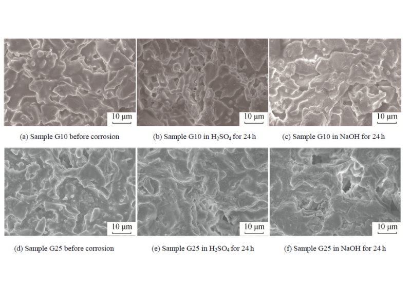
Silicon Carbide (SiC) porous ceramic supports are widely used in advanced membrane filtration systems due to their excellent thermal stability, high mechanical strength, and superior chemical resistance. SiC-based ceramic materials are especially suitable for harsh environments such as high-temperature filtration, wastewater treatment, and chemical processing. However, conventional SiC ceramics require extremely high sintering temperatures (>2000°C), limiting large-scale industrial production. To address this challenge, low-temperature liquid-phase sintering using glass additives has become an effective solution. Low-Temperature Sintering Strategy for SiC Ceramics In this study, a zirconium-containing glass frit derived from low-cost shale was introduced as a sintering aid to promote liquid-phase bonding and reduce sintering temperature significantly. The glass frit is

多孔質炭化ケイ素(SiC)セラミック担体:低温焼結技術と性能に関する研究 続きを読む »

炭化ケイ素セラミックス:過酷な産業環境向けの先端エンジニアリング材料

As industrial equipment continues to evolve toward higher precision, higher temperatures, and more demanding operating conditions, conventional materials such as metals and standard ceramics are increasingly reaching their performance limits. Wear, thermal deformation, chemical corrosion, particle contamination, and electrical instability can all negatively impact manufacturing efficiency, product quality, and equipment lifespan. Among advanced engineering materials, Silicon Carbide (SiC) ceramics have emerged as one of the most important solutions for addressing these challenges. Thanks to their exceptional combination of mechanical, thermal, chemical, and electrical properties, SiC ceramics are widely used in semiconductor manufacturing, industrial processing, energy systems, chemical equipment, and precision machinery. But what makes silicon carbide so special, and why

炭化ケイ素セラミックス:過酷な産業環境向けの先端エンジニアリング材料 続きを読む »

hBNが次世代2次元材料の開発をどのように可能にするか

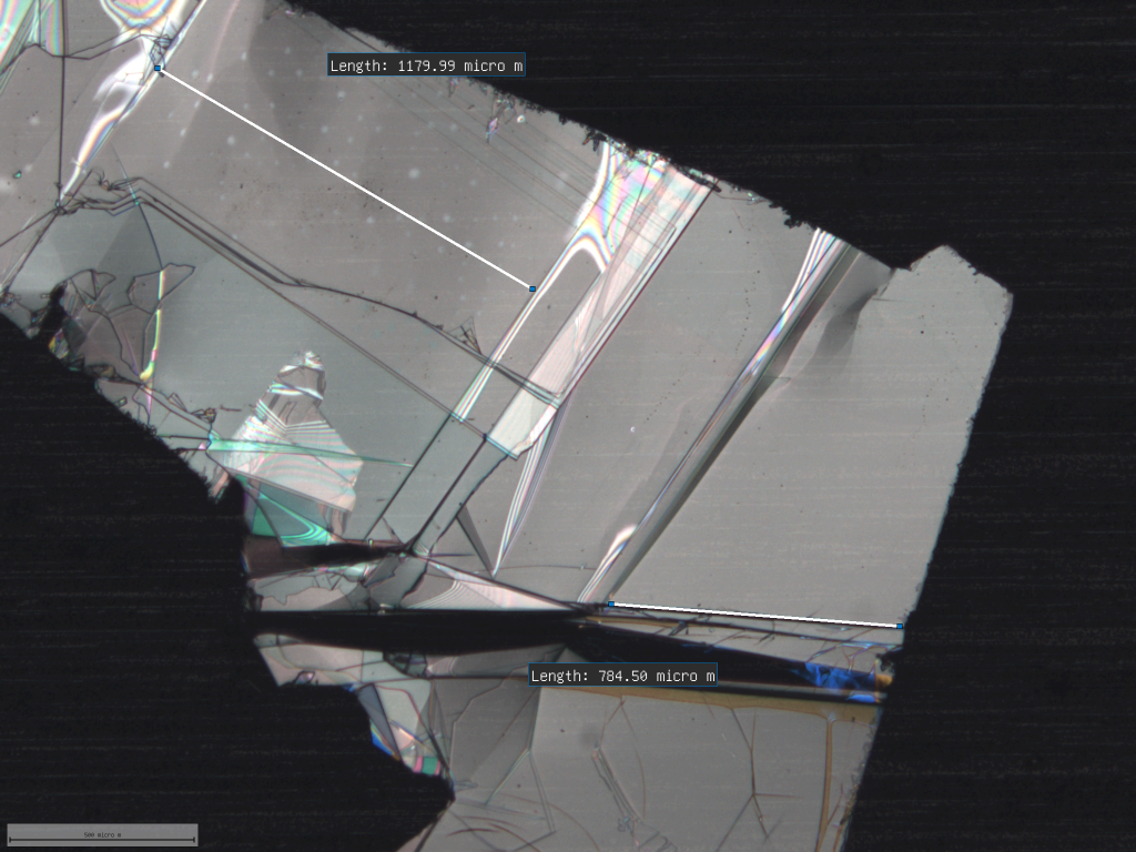
The rapid expansion of two-dimensional (2D) materials research has opened entirely new directions in electronics, photonics, and quantum technologies. Materials such as graphene, transition metal dichalcogenides (TMDs), and other atomically thin crystals exhibit extraordinary properties that differ fundamentally from their bulk counterparts. However, the practical realization of high-performance 2D devices depends not only on the active material itself, but also critically on the surrounding environment. In this context, hexagonal boron nitride (hBN) single crystals have emerged as one of the most important enabling materials for next-generation 2D systems. The Challenge of Building 2D Material Devices Unlike conventional semiconductors, 2D materials are only one or a few atomic layers thick. This

hBNが次世代2次元材料の開発をどのように可能にするか 続きを読む »

デバイスグレードのhBNが、将来の半導体における戦略的素材となりつつある理由

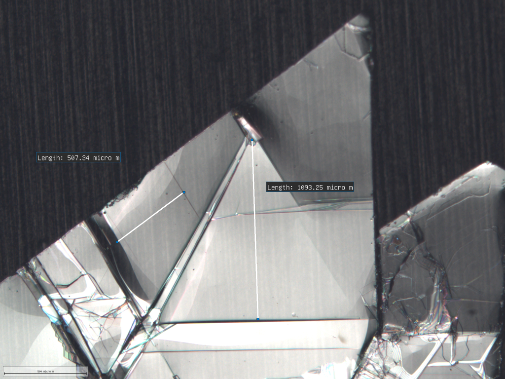
As semiconductor technology continues to scale beyond traditional silicon-based architectures, the industry is increasingly turning toward new classes of materials that can support higher performance, lower power consumption, and fundamentally new device physics. Among these emerging materials, device-grade hexagonal boron nitride (hBN) single crystal has rapidly gained attention as a strategic enabler for next-generation electronics. Once considered a niche laboratory material, hBN is now recognized as a critical component in advanced semiconductor research, particularly in two-dimensional (2D) electronics, quantum devices, and van der Waals heterostructures. The Semiconductor Industry Is Facing Fundamental Limits Modern semiconductor scaling is approaching physical and material constraints. As device dimensions shrink, several challenges become increasingly severe:

デバイスグレードのhBNが、将来の半導体における戦略的素材となりつつある理由 続きを読む »

グラフェンとhBN:2次元エレクトロニクスにおける最も重要な組み合わせ

In the rapidly evolving field of two-dimensional (2D) materials, few material combinations have had as profound an impact as graphene and hexagonal boron nitride (hBN). While graphene is celebrated for its extraordinary electrical, mechanical, and thermal properties, its full potential can only be realized when paired with an equally remarkable companion: high-quality hBN single crystals. Together, graphene and hBN form the foundation of modern 2D electronics, enabling breakthroughs in nanoelectronics, quantum transport, and van der Waals heterostructure engineering. Graphene: A Powerful but Environment-Sensitive Material Graphene is a single layer of carbon atoms arranged in a hexagonal lattice. It exhibits exceptional properties, including: However, graphene’s biggest limitation is not its intrinsic

グラフェンとhBN:2次元エレクトロニクスにおける最も重要な組み合わせ 続きを読む »

高移動度グラフェンデバイスがhBN単結晶に依存する理由

Graphene is widely regarded as one of the most remarkable materials ever discovered. Its exceptional electrical conductivity, mechanical strength, and atomic thickness have opened new possibilities in nanoelectronics, sensing, and quantum technologies. However, one of the most important discoveries in graphene research is that its performance is not solely determined by graphene itself—but critically depends on the underlying substrate material. Among all known substrate materials, hexagonal boron nitride (hBN) single crystal has proven to be the most effective platform for achieving high-mobility graphene devices. This article explains why hBN single crystals are essential for unlocking graphene’s true electronic potential. The Challenge: Graphene Is Extremely Sensitive to Its Environment Although graphene

高移動度グラフェンデバイスがhBN単結晶に依存する理由 続きを読む »