xinkehui

Ceramic Wafer End Effector Design: Material, Weight, Flatness and Particle Control

A ceramic wafer end effector—also called a wafer handling blade, robot blade or wafer transfer arm—is the part of a semiconductor robot that directly supports and transfers wafers between process chambers, load ports, aligners, inspection stations and wafer carriers. Although its geometry may appear simple, the end effector directly affects wafer positioning accuracy, transfer speed, […]

Ceramic Wafer End Effector Design: Material, Weight, Flatness and Particle Control Číst více »
Wafer Chucking Force: Vacuum Pressure, Contact Area and Wafer Flatness

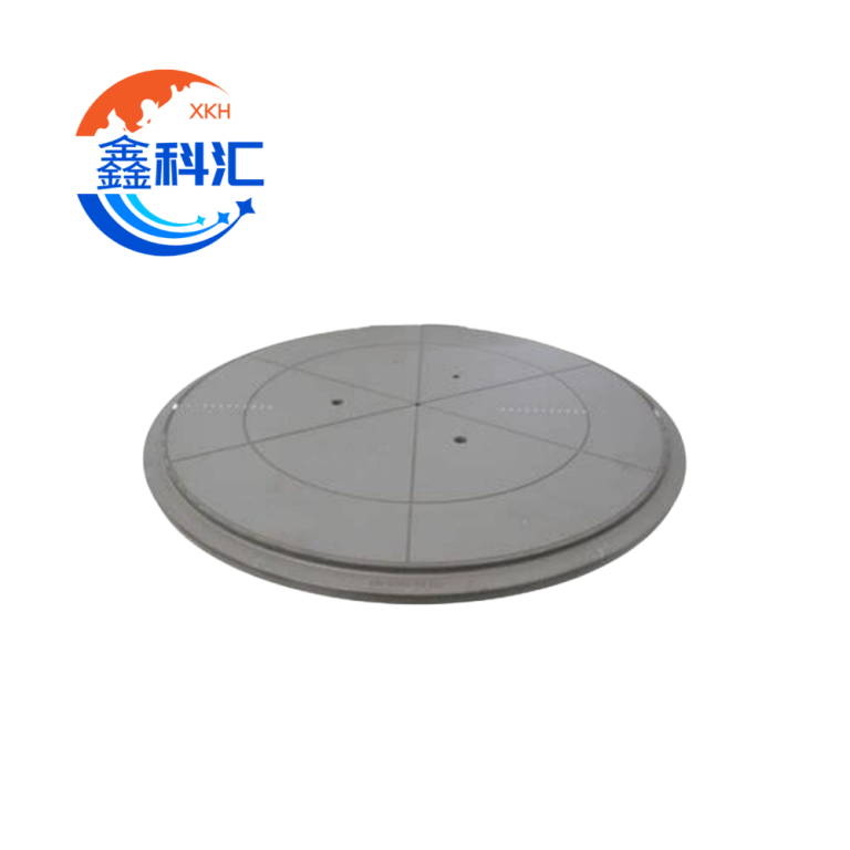
Wafer chucking force is one of the most important design parameters in semiconductor wafer handling, inspection, lithography, grinding, coating and precision machining equipment. A vacuum chuck must hold the wafer securely against acceleration, vibration and process loads. At the same time, it must avoid excessive local stress, backside contamination, wafer deformation and imprinting of the

Wafer Chucking Force: Vacuum Pressure, Contact Area and Wafer Flatness Číst více »

Ceramic Wafer Support Pins: Material Selection, Flatness and Particle Control

Ceramic wafer support pins are small but critical components in semiconductor processing equipment. They support, lift, position or temporarily separate wafers during transfer between a robot arm, process chamber, electrostatic chuck, vacuum chuck or wafer stage. Although their geometry is relatively simple, wafer support pins directly contact or approach sensitive wafer surfaces. Variations in pin

Ceramic Wafer Support Pins: Material Selection, Flatness and Particle Control Číst více »
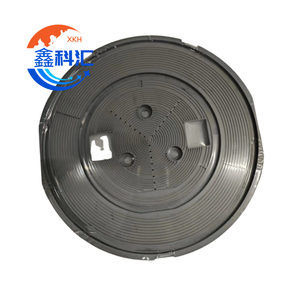
Ceramic Vacuum Chuck Design: Porosity, Flatness and Wafer Holding Performance

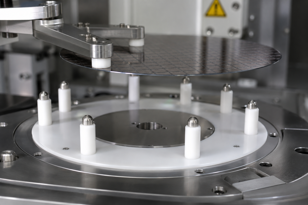
Vacuum chucks are essential components in modern semiconductor manufacturing. They securely hold silicon, silicon carbide (SiC), sapphire, glass, and compound semiconductor wafers during lithography, inspection, grinding, polishing, laser processing, metrology, and wafer bonding. Among various chuck technologies, porous ceramic vacuum chuck have become the preferred solution because they provide uniform vacuum distribution, excellent dimensional stability,

Ceramic Vacuum Chuck Design: Porosity, Flatness and Wafer Holding Performance Číst více »

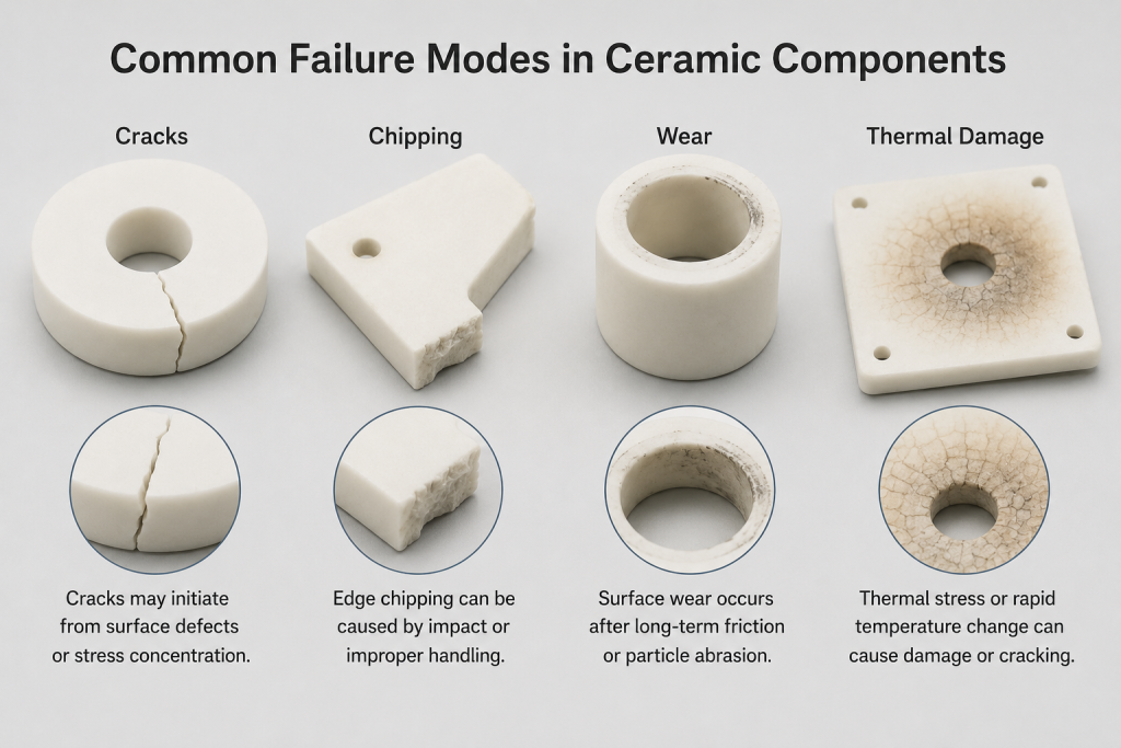
Ceramic Components Failure Analysis: Cracks, Chipping, Wear and Thermal Damage

Advanced ceramic components are widely used in semiconductor equipment, vacuum systems, precision machinery, electrical insulation, chemical processing and high-temperature applications. Materials such as alumina, zirconia, aluminum nitride, silicon carbide and silicon nitride provide excellent hardness, wear resistance, corrosion resistance, electrical insulation and dimensional stability. Despite these advantages, ceramic components can still fail. Unlike most metals,

Ceramic Components Failure Analysis: Cracks, Chipping, Wear and Thermal Damage Číst více »

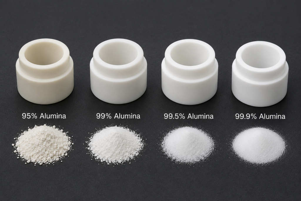
Alumina Ceramic Purity Levels Explained: 95%, 99%, 99.5% and 99.9% Compared

Alumina ceramic, also known as aluminum oxide ceramic or Al₂O₃ ceramic, is one of the most widely used technical ceramic materials. It offers a practical combination of electrical insulation, mechanical strength, hardness, wear resistance, thermal stability and corrosion resistance. However, not all alumina ceramics are the same. Commercial alumina materials are commonly identified by their

Alumina Ceramic Purity Levels Explained: 95%, 99%, 99.5% and 99.9% Compared Číst více »

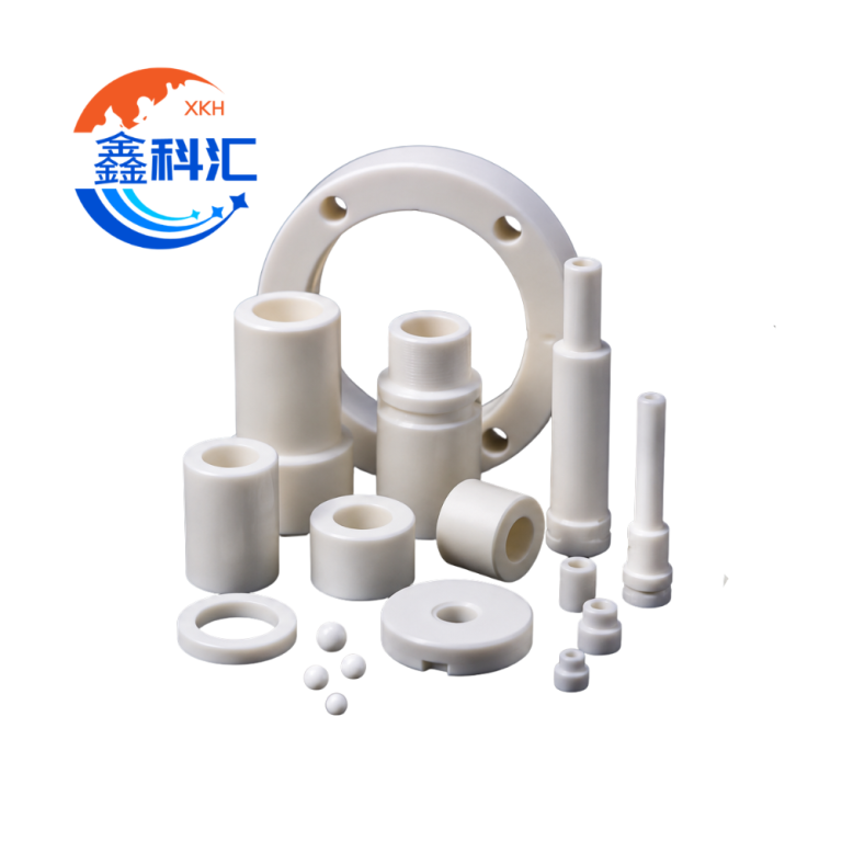
Structural Ceramics for Semiconductor Manufacturing: Key Materials and Equipment Applications

Semiconductor manufacturing requires materials that can operate reliably under high temperature, plasma exposure, chemical corrosion, vacuum conditions and strict cleanliness requirements. In many process tools, metal and plastic components cannot meet these demanding conditions. This is why structural ceramics are widely used in semiconductor equipment. Structural ceramics are advanced ceramic materials designed to provide mechanical

Structural Ceramics for Semiconductor Manufacturing: Key Materials and Equipment Applications Číst více »

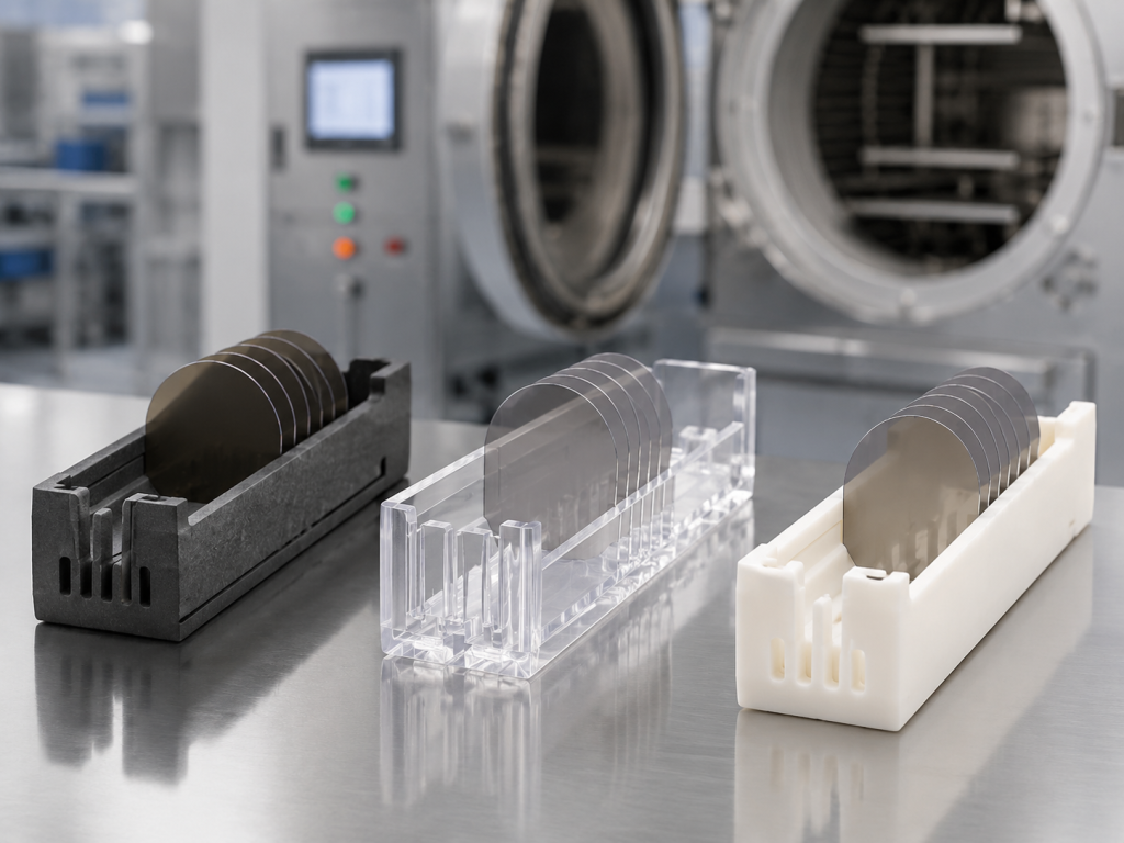
Semiconductor Wafer Boat Materials: SiC, Quartz and Alumina Compared

In semiconductor manufacturing, wafer boats are used to hold and support wafers during high-temperature processes such as diffusion, oxidation, annealing and LPCVD. Although the structure of a wafer boat may look simple, the material choice is very important. Different materials can affect thermal stability, contamination control, mechanical strength, service life and overall process reliability. Among

Semiconductor Wafer Boat Materials: SiC, Quartz and Alumina Compared Číst více »

Co je to loďka na polovodičové destičky? Materiály, konstrukce a použití

In semiconductor manufacturing, wafers must be processed, transported, heated and cooled under highly controlled conditions. During high-temperature processes such as diffusion, oxidation, annealing and LPCVD, wafers cannot simply be placed directly inside a furnace. They need a stable, clean and precisely designed carrier to hold them in position. This carrier is commonly known as a

Co je to loďka na polovodičové destičky? Materiály, konstrukce a použití Číst více »

Keramické substráty: Základní prvek řízení tepla v moderních elektronických zařízeních

S tím, jak se nové technologie, jako jsou elektromobily (EV), komunikace 5G, systémy využívající obnovitelné zdroje energie, umělá inteligence (AI), letecká elektronika a výkonové polovodiče, neustále vyvíjejí, stávají se elektronická zařízení stále výkonnějšími, kompaktnějšími a vysoce integrovanými. Ačkoli tyto pokroky zlepšují výkon, zároveň generují výrazně vyšší tepelnou hustotu, což představuje zásadní výzvy pro řízení tepla a spolehlivost zařízení.

Keramické substráty: Základní prvek řízení tepla v moderních elektronických zařízeních Číst více »

Pokročilé keramické materiály v polovodičové optoelektronice: aplikace, výhody a budoucí perspektivy

As semiconductor and optoelectronic technologies continue to advance toward higher power, greater integration, and improved reliability, the demand for high-performance materials is growing rapidly. Among the many advanced materials used in modern optoelectronic devices, ceramic materials have emerged as a critical enabling technology due to their exceptional thermal stability, chemical resistance, electrical insulation, and optical

Pokročilé keramické materiály v polovodičové optoelektronice: aplikace, výhody a budoucí perspektivy Číst více »

Overcoming the Challenges of Manufacturing Complex Semiconductor Ceramic Components

Advanced ceramics have become indispensable materials in modern semiconductor equipment. Components used in plasma etching, chemical vapor deposition (CVD), physical vapor deposition (PVD), ion implantation, and wafer handling systems must operate reliably under extreme conditions, including high-energy plasma exposure, corrosive process gases, elevated temperatures, thermal cycling, and high-voltage electrical fields. Materials such as alumina (Al₂O₃),

Overcoming the Challenges of Manufacturing Complex Semiconductor Ceramic Components Číst více »