業界ニュース

Alumina Ceramic Multi-Hole Plate Design: Hole Diameter, Pitch, Flatness and Inspection

Alumina ceramic multi-hole plates are used in semiconductor equipment, gas distribution systems, vacuum fixtures, electrical insulation assemblies, filtration supports, furnace components and precision industrial machinery. Although the basic structure may appear simple, manufacturing hundreds or thousands of accurately positioned holes in a ceramic plate requires careful control of hole diameter, pitch, true position, plate thickness, flatness and edge quality. A small change in hole diameter can affect gas flow or pressure drop. Accumulated pitch error may prevent the plate from aligning with other components, while excessive flatness variation can create sealing gaps or uneven mechanical loading. A complete RFQ should therefore define both the individual hole requirements and the overall […]

Alumina Ceramic Multi-Hole Plate Design: Hole Diameter, Pitch, Flatness and Inspection 続きを読む »
Zirconia Ceramic Parts Tolerance Guide: Dimensional Accuracy, Surface Finish and Inspection

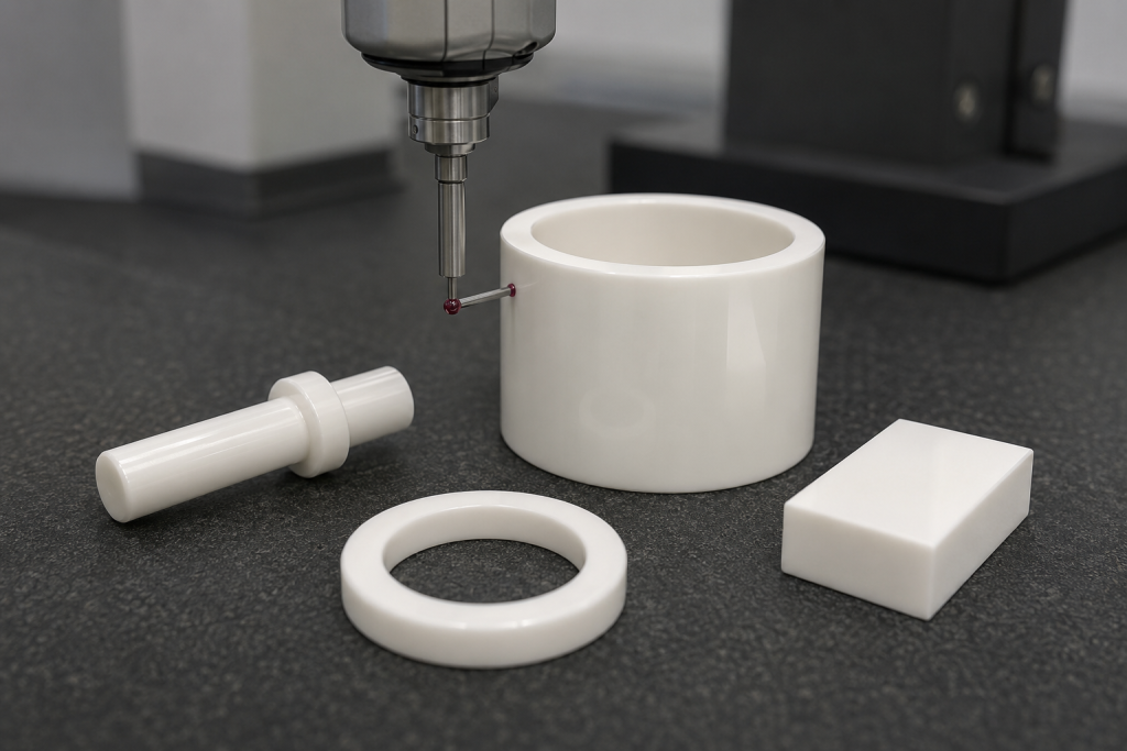
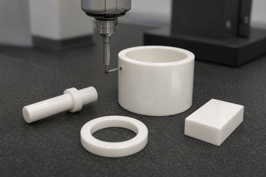
Zirconia ceramic parts are widely used in applications requiring high strength, fracture toughness, wear resistance, electrical insulation and a smooth working surface. Typical products include ceramic shafts, sleeves, bushings, plungers, valve components, positioning pins, guides, nozzles and semiconductor equipment parts. However, specifying a zirconia component cannot be handled in exactly the same way as specifying a metal part. Zirconia is formed, sintered and often diamond-ground after firing. Sintering shrinkage, part geometry, grinding access, wall thickness and inspection methods all affect the tolerances that can be achieved. A good zirconia drawing should identify the dimensions that are functionally critical, the surfaces that require grinding or polishing, the required geometric tolerances and

Zirconia Ceramic Parts Tolerance Guide: Dimensional Accuracy, Surface Finish and Inspection 続きを読む »

カスタムウェーハボートの指定方法:ウェーハ径、スロットピッチ、収容数、および公差

A custom wafer boat must do more than hold a group of wafers. It must maintain consistent wafer spacing, fit the processing equipment, withstand repeated thermal cycles and avoid introducing particles or metallic contamination. Small dimensional errors can create serious operating problems. Incorrect slot pitch may interfere with robotic loading, insufficient clearance can damage wafer edges, and excessive deformation may cause wafers to lean or contact each other during high-temperature processing. For this reason, a reliable wafer boat RFQ should define the wafer, process, equipment interface, slot geometry, capacity, material, dimensional tolerances and inspection requirements. What Is a Semiconductor Wafer Boat? A wafer boat is a precision carrier used to

カスタムウェーハボートの指定方法:ウェーハ径、スロットピッチ、収容数、および公差 続きを読む »

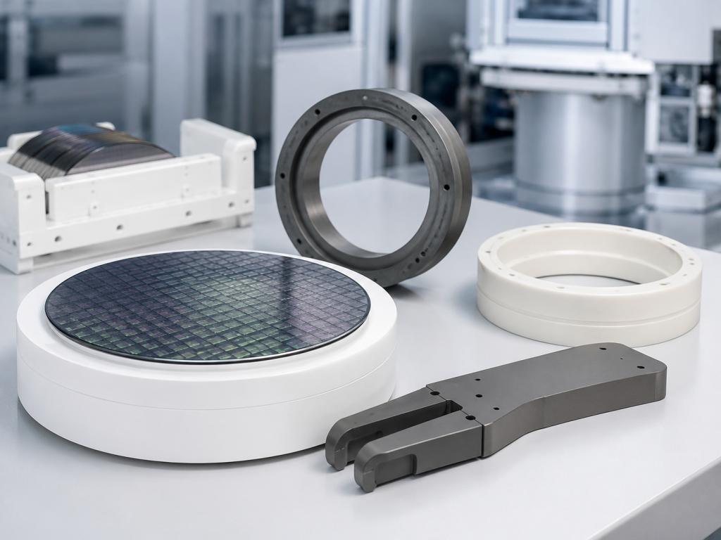
半導体製造用構造用セラミックス:構成部品および材料の選定

Structural ceramics play a critical role in semiconductor manufacturing equipment because many process components must operate under conditions that are difficult for conventional metals and polymers. Depending on the process, equipment parts may be exposed to: Advanced ceramics are used in wafer handling, lithography, etching, deposition, thermal processing, cleaning, inspection, back grinding and other semiconductor processes. Ceramic components commonly include vacuum chucks, electrostatic chuck parts, end effectors, focus rings, chamber liners, nozzles, showerheads, heater components, wafer boats and precision stage structures. However, “ceramic” is not a single material specification. Alumina, silicon carbide, aluminum nitride, silicon nitride, zirconia, yttria and cordierite have very different mechanical, thermal, electrical and plasma-resistance characteristics. Material

半導体製造用構造用セラミックス:構成部品および材料の選定 続きを読む »

ウェーハのチャッキング力:真空圧力、接触面積、およびウェーハの平坦度

Wafer chucking force is one of the most important design parameters in semiconductor wafer handling, inspection, lithography, grinding, coating and precision machining equipment. A vacuum chuck must hold the wafer securely against acceleration, vibration and process loads. At the same time, it must avoid excessive local stress, backside contamination, wafer deformation and imprinting of the chuck surface pattern. Increasing vacuum pressure does not automatically produce better wafer positioning. The final result depends on the interaction between: Vacuum wafer chucks are widely used for wafer holding during processes including lithography, spin coating, etching, inspection and metrology. Ceramic chuck materials are often selected because they can provide high stiffness, dimensional stability, low

ウェーハのチャッキング力:真空圧力、接触面積、およびウェーハの平坦度 続きを読む »

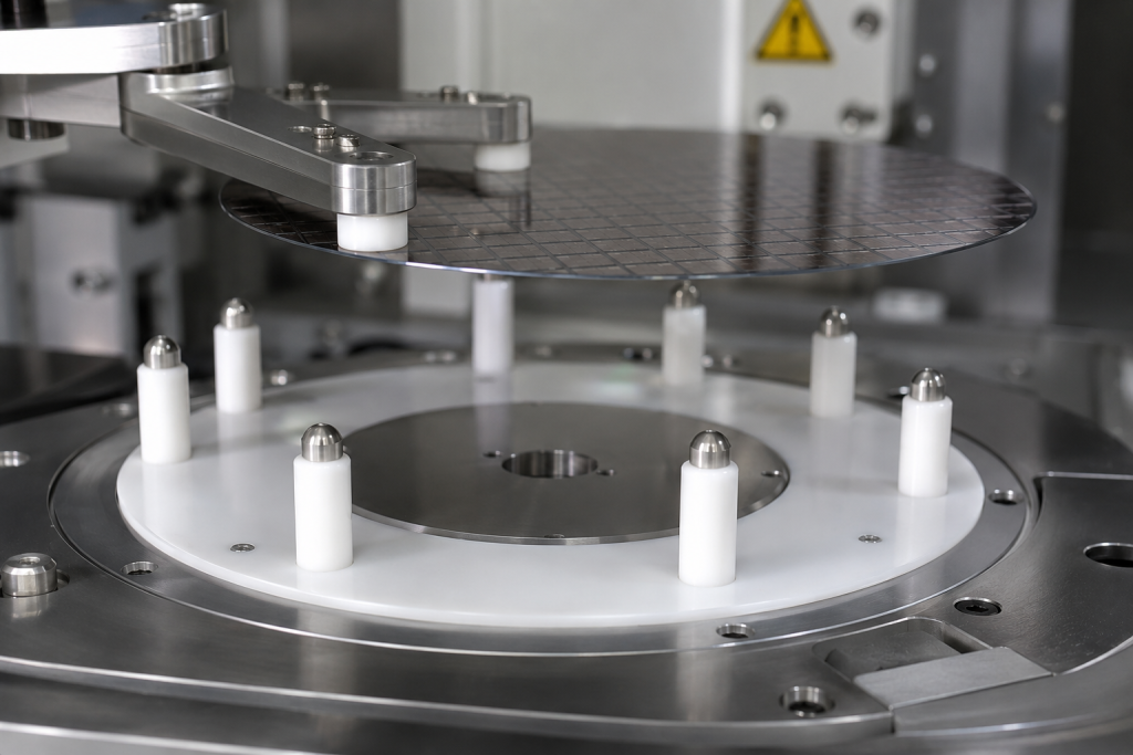
セラミックウェーハ用支持ピン:材料選定、平坦度および粒子管理

Ceramic wafer support pins are small but critical components in semiconductor processing equipment. They support, lift, position or temporarily separate wafers during transfer between a robot arm, process chamber, electrostatic chuck, vacuum chuck or wafer stage. Although their geometry is relatively simple, wafer support pins directly contact or approach sensitive wafer surfaces. Variations in pin height, tip geometry, material quality or surface cleanliness can therefore lead to wafer tilt, localized stress, scratches, particles and positioning errors. As silicon, silicon carbide, sapphire, gallium nitride and other semiconductor wafers become thinner and more valuable, the design and manufacturing quality of support pins become increasingly important. This article explains how material selection, height

セラミックウェーハ用支持ピン:材料選定、平坦度および粒子管理 続きを読む »

セラミック真空チャックの設計:気孔率、平坦度、およびウェーハ保持性能

Vacuum chucks are essential components in modern semiconductor manufacturing. They securely hold silicon, silicon carbide (SiC), sapphire, glass, and compound semiconductor wafers during lithography, inspection, grinding, polishing, laser processing, metrology, and wafer bonding. Among various chuck technologies, porous ceramic vacuum chuck have become the preferred solution because they provide uniform vacuum distribution, excellent dimensional stability, high cleanliness, and outstanding wear resistance. However, not all ceramic vacuum chucks deliver the same performance. Their ability to securely hold ultra-flat wafers depends on several engineering parameters, including porosity, flatness, material selection, vacuum distribution, and machining accuracy. This article explains how these design factors influence wafer holding performance and what engineers should consider when

セラミック真空チャックの設計:気孔率、平坦度、およびウェーハ保持性能 続きを読む »

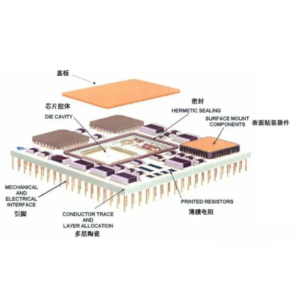
セラミック基板:先端電子デバイスの熱管理を支える中核技術

As emerging technologies such as electric vehicles (EVs), 5G communications, renewable energy systems, artificial intelligence (AI), aerospace electronics, and power semiconductors continue to evolve, electronic devices are becoming increasingly powerful, compact, and highly integrated. While these advancements improve performance, they also generate significantly higher heat densities, creating critical challenges for thermal management and device reliability. Efficient heat dissipation has become one of the most important factors determining the lifespan, performance, and safety of modern electronic systems. Among various packaging and thermal management materials, ceramic substrates have emerged as indispensable components due to their unique combination of high thermal conductivity, excellent electrical insulation, mechanical strength, and chemical stability. Today, ceramic substrates

セラミック基板:先端電子デバイスの熱管理を支える中核技術 続きを読む »

6つの主要なセラミック基板材料を解説:完全ガイド

With the rapid development of electric vehicles, power electronics, aerospace systems, satellite communications, and high-frequency semiconductor devices, electronic components are increasingly required to operate under high power, high temperature, and high frequency conditions. In such demanding environments, traditional organic or metal-based substrates often fail to provide sufficient thermal and electrical stability. As a result, advanced ceramic substrates have become essential in modern electronic packaging and thermal management systems. Ceramic substrates offer excellent thermal conductivity, electrical insulation, mechanical strength, and long-term reliability, making them ideal for next-generation high-performance devices. This article introduces the six most important ceramic substrate materials used in advanced electronics today. 1. Aluminum Oxide (Al₂O₃) Ceramic Substrate Aluminum

6つの主要なセラミック基板材料を解説:完全ガイド 続きを読む »

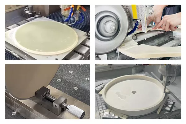
半導体セラミック部品製造プロセス:原料粉末から精密部品まで

Modern semiconductor manufacturing relies heavily on advanced equipment such as etching systems, lithography machines, ion implantation tools, and deposition equipment. Inside these systems, numerous ceramic components play critical roles in ensuring process stability, precision, and reliability. Thanks to their exceptional high-temperature resistance, corrosion resistance, mechanical strength, dimensional stability, and electrical properties, advanced ceramic components are widely used throughout semiconductor fabrication processes. Many of these components come into direct contact with wafers and are responsible for precise temperature control, plasma resistance, vacuum handling, and contamination reduction. Common semiconductor ceramic materials include: Typical semiconductor ceramic components include: The manufacturing of semiconductor ceramic parts involves a series of highly controlled processes, including powder

半導体セラミック部品製造プロセス:原料粉末から精密部品まで 続きを読む »

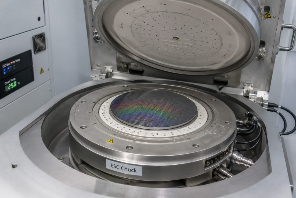
静電チャック vs 真空チャック:半導体製造におけるウェーハ保持技術はどちらが優れているか?

In semiconductor manufacturing, wafer positioning and fixation are fundamental requirements for achieving process precision and yield stability. During etching, deposition, lithography, inspection, and plasma processing, silicon wafers must remain securely held while maintaining minimal contamination and excellent thermal uniformity. As device structures continue shrinking and wafer sizes continue increasing, traditional holding methods face growing challenges. Two of the most widely used wafer fixation technologies today are Electrostatic Chucks (ESCs) and Vacuum Chucks. Although both systems serve the same general purpose—holding wafers in place—their working principles, operating environments, and performance characteristics differ significantly. Understanding these differences is essential for equipment designers, process engineers, and semiconductor manufacturers. Why Wafer Holding Technology Matters

静電チャック vs 真空チャック:半導体製造におけるウェーハ保持技術はどちらが優れているか? 続きを読む »

炭化ケイ素トレイが従来のウェハーキャリアに取って代わる理由

As semiconductor manufacturing continues moving toward larger wafer sizes, higher process temperatures, and stricter contamination standards, conventional wafer carrier materials are increasingly reaching their performance limits. Components that once met process requirements are now facing challenges involving thermal deformation, particle generation, and shorter service life. Among advanced ceramic materials, silicon carbide (SiC) trays have emerged as one of the most promising alternatives to traditional wafer carriers. Thanks to their superior thermal, mechanical, and chemical properties, SiC trays are increasingly being adopted in semiconductor processing equipment. But what is driving this shift? Why are silicon carbide trays gradually replacing conventional wafer carriers in high-end semiconductor manufacturing? This article explores the material

炭化ケイ素トレイが従来のウェハーキャリアに取って代わる理由 続きを読む »