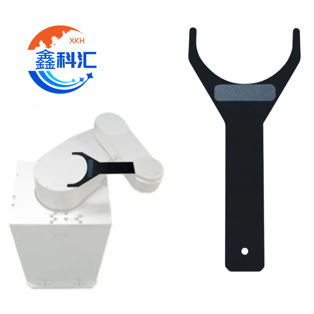
アドバンスト・セラミックスはいかにして半導体装置の性能を向上させるか
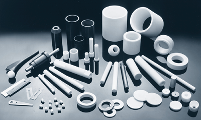
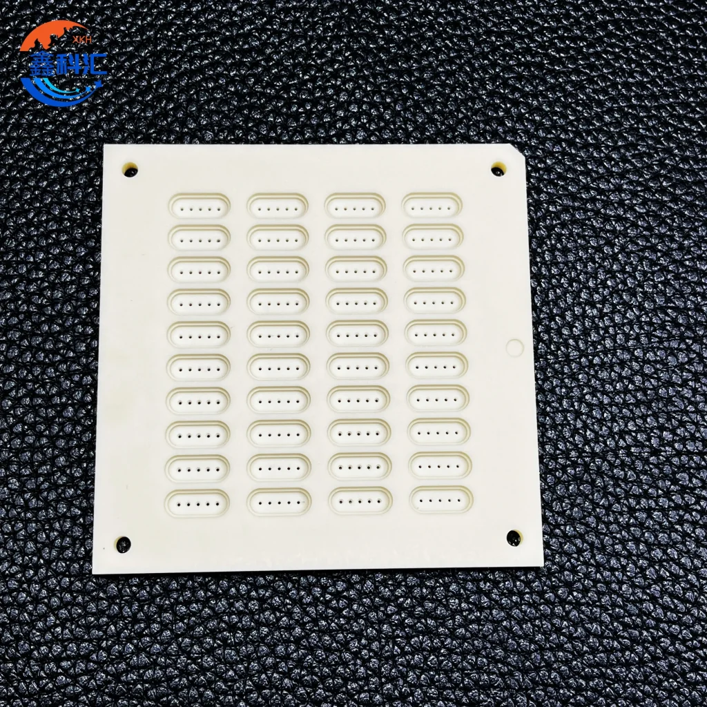
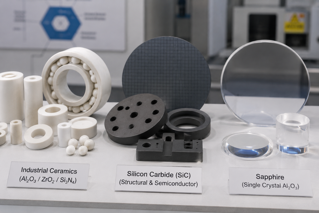
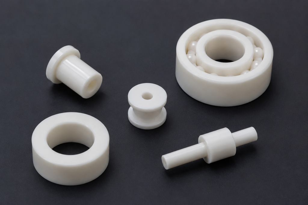
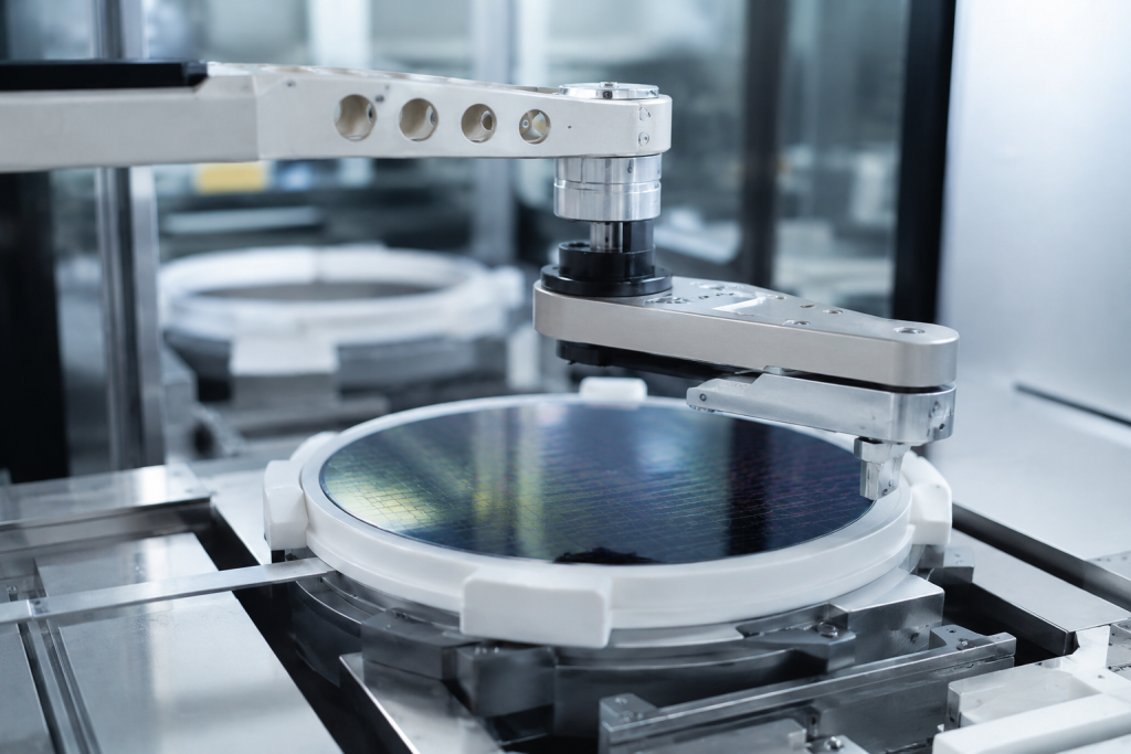
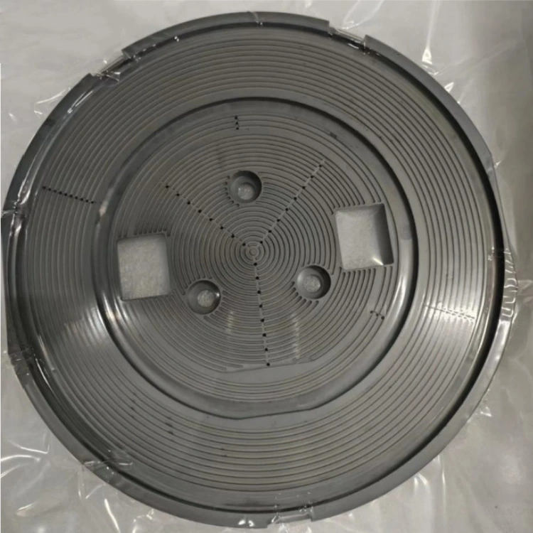
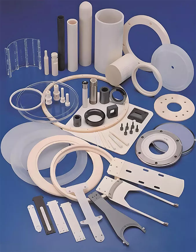
The semiconductor industry operates at the limits of precision engineering. Modern fabrication processes require extreme temperatures, highly reactive chemicals, plasma exposure, vacuum environments, and contamination control at microscopic scales. As integrated circuits continue advancing toward smaller process nodes and larger wafer sizes, equipment performance requirements become increasingly demanding. Under these conditions, material selection becomes a critical factor influencing manufacturing yield, process stability, and equipment lifetime. Traditional metallic materials often struggle to satisfy the severe environmental requirements found inside semiconductor systems. Consequently, advanced ceramics have emerged as indispensable materials in semiconductor equipment. Through their exceptional thermal stability, chemical resistance, mechanical strength, and low contamination characteristics, advanced ceramics significantly improve the performance […]
アドバンスト・セラミックスはいかにして半導体装置の性能を向上させるか 続きを読む »