Nouvelles de l'industrie

Alumina Ceramic Multi-Hole Plate Design: Hole Diameter, Pitch, Flatness and Inspection

Alumina ceramic multi-hole plates are used in semiconductor equipment, gas distribution systems, vacuum fixtures, electrical insulation assemblies, filtration supports, furnace components and precision industrial machinery. Although the basic structure may appear simple, manufacturing hundreds or thousands of accurately positioned holes in a ceramic plate requires careful control of hole diameter, pitch, true position, plate thickness, […]

Alumina Ceramic Multi-Hole Plate Design: Hole Diameter, Pitch, Flatness and Inspection Lire la suite »

Zirconia Ceramic Parts Tolerance Guide: Dimensional Accuracy, Surface Finish and Inspection

Zirconia ceramic parts are widely used in applications requiring high strength, fracture toughness, wear resistance, electrical insulation and a smooth working surface. Typical products include ceramic shafts, sleeves, bushings, plungers, valve components, positioning pins, guides, nozzles and semiconductor equipment parts. However, specifying a zirconia component cannot be handled in exactly the same way as specifying

Zirconia Ceramic Parts Tolerance Guide: Dimensional Accuracy, Surface Finish and Inspection Lire la suite »

How to Specify a Custom Wafer Boat: Wafer Diameter, Slot Pitch, Capacity and Tolerances

A custom wafer boat must do more than hold a group of wafers. It must maintain consistent wafer spacing, fit the processing equipment, withstand repeated thermal cycles and avoid introducing particles or metallic contamination. Small dimensional errors can create serious operating problems. Incorrect slot pitch may interfere with robotic loading, insufficient clearance can damage wafer

How to Specify a Custom Wafer Boat: Wafer Diameter, Slot Pitch, Capacity and Tolerances Lire la suite »

Structural Ceramics for Semiconductor Manufacturing: Component and Material Selection

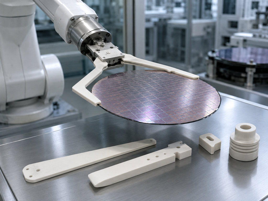
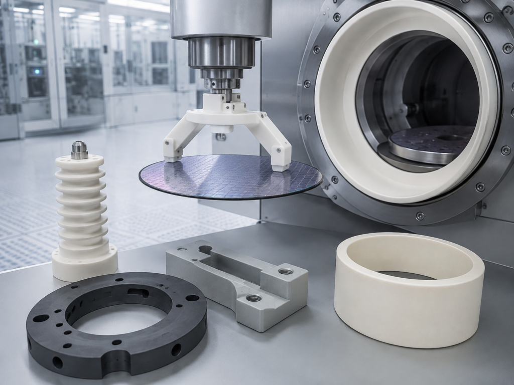
Structural ceramics play a critical role in semiconductor manufacturing equipment because many process components must operate under conditions that are difficult for conventional metals and polymers. Depending on the process, equipment parts may be exposed to: Advanced ceramics are used in wafer handling, lithography, etching, deposition, thermal processing, cleaning, inspection, back grinding and other semiconductor

Structural Ceramics for Semiconductor Manufacturing: Component and Material Selection Lire la suite »

Wafer Chucking Force: Vacuum Pressure, Contact Area and Wafer Flatness

Wafer chucking force is one of the most important design parameters in semiconductor wafer handling, inspection, lithography, grinding, coating and precision machining equipment. A vacuum chuck must hold the wafer securely against acceleration, vibration and process loads. At the same time, it must avoid excessive local stress, backside contamination, wafer deformation and imprinting of the

Wafer Chucking Force: Vacuum Pressure, Contact Area and Wafer Flatness Lire la suite »

Ceramic Wafer Support Pins: Material Selection, Flatness and Particle Control

Ceramic wafer support pins are small but critical components in semiconductor processing equipment. They support, lift, position or temporarily separate wafers during transfer between a robot arm, process chamber, electrostatic chuck, vacuum chuck or wafer stage. Although their geometry is relatively simple, wafer support pins directly contact or approach sensitive wafer surfaces. Variations in pin

Ceramic Wafer Support Pins: Material Selection, Flatness and Particle Control Lire la suite »

Ceramic Vacuum Chuck Design: Porosity, Flatness and Wafer Holding Performance

Vacuum chucks are essential components in modern semiconductor manufacturing. They securely hold silicon, silicon carbide (SiC), sapphire, glass, and compound semiconductor wafers during lithography, inspection, grinding, polishing, laser processing, metrology, and wafer bonding. Among various chuck technologies, porous ceramic vacuum chuck have become the preferred solution because they provide uniform vacuum distribution, excellent dimensional stability,

Ceramic Vacuum Chuck Design: Porosity, Flatness and Wafer Holding Performance Lire la suite »

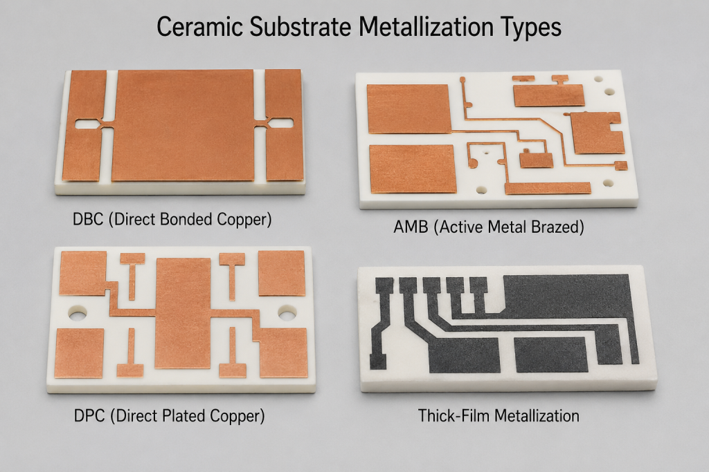
Ceramic Substrates: The Thermal Management Backbone of Advanced Electronic Devices

As emerging technologies such as electric vehicles (EVs), 5G communications, renewable energy systems, artificial intelligence (AI), aerospace electronics, and power semiconductors continue to evolve, electronic devices are becoming increasingly powerful, compact, and highly integrated. While these advancements improve performance, they also generate significantly higher heat densities, creating critical challenges for thermal management and device reliability.

Ceramic Substrates: The Thermal Management Backbone of Advanced Electronic Devices Lire la suite »

Les 6 principaux matériaux de substrat céramique expliqués : un guide complet

With the rapid development of electric vehicles, power electronics, aerospace systems, satellite communications, and high-frequency semiconductor devices, electronic components are increasingly required to operate under high power, high temperature, and high frequency conditions. In such demanding environments, traditional organic or metal-based substrates often fail to provide sufficient thermal and electrical stability. As a result, advanced

Les 6 principaux matériaux de substrat céramique expliqués : un guide complet Lire la suite »

Processus de fabrication des composants céramiques pour semi-conducteurs : De la poudre brute aux pièces de précision

Modern semiconductor manufacturing relies heavily on advanced equipment such as etching systems, lithography machines, ion implantation tools, and deposition equipment. Inside these systems, numerous ceramic components play critical roles in ensuring process stability, precision, and reliability. Thanks to their exceptional high-temperature resistance, corrosion resistance, mechanical strength, dimensional stability, and electrical properties, advanced ceramic components are

Processus de fabrication des composants céramiques pour semi-conducteurs : De la poudre brute aux pièces de précision Lire la suite »

Mandrin électrostatique ou mandrin à vide : quelle est la meilleure technologie de maintien des wafers pour la fabrication de semi-conducteurs ?

In semiconductor manufacturing, wafer positioning and fixation are fundamental requirements for achieving process precision and yield stability. During etching, deposition, lithography, inspection, and plasma processing, silicon wafers must remain securely held while maintaining minimal contamination and excellent thermal uniformity. As device structures continue shrinking and wafer sizes continue increasing, traditional holding methods face growing challenges.

Mandrin électrostatique ou mandrin à vide : quelle est la meilleure technologie de maintien des wafers pour la fabrication de semi-conducteurs ? Lire la suite »

Pourquoi les plateaux en carbure de silicium remplacent-ils les supports de plaquettes traditionnels ?

As semiconductor manufacturing continues moving toward larger wafer sizes, higher process temperatures, and stricter contamination standards, conventional wafer carrier materials are increasingly reaching their performance limits. Components that once met process requirements are now facing challenges involving thermal deformation, particle generation, and shorter service life. Among advanced ceramic materials, silicon carbide (SiC) trays have emerged

Pourquoi les plateaux en carbure de silicium remplacent-ils les supports de plaquettes traditionnels ? Lire la suite »