業界ニュース

セラミック真空チャック

半導体製造における多孔質セラミックス:高度な材料設計による高精度の実現

Porous ceramics are engineered ceramic materials produced through specialized processing techniques that create interconnected or closed pore structures within the material. Their porosity typically ranges from 20% to 90%, while pore sizes can vary from nanometer scale to millimeter scale depending on design requirements. Thanks to their unique internal architecture and outstanding physical properties—including high-temperature resistance, corrosion resistance, excellent insulation, and structural stability—porous ceramics have become increasingly important in semiconductor manufacturing. These materials play a critical role in improving process precision, production yield, and equipment reliability across multiple semiconductor applications. Among their many uses, one of the most significant applications is in ceramic vacuum chucks. What Makes Porous Ceramics Unique? […]

半導体製造における多孔質セラミックス:高度な材料設計による高精度の実現 続きを読む »
半導体セラミックスの解説:現代技術を変える機能性電子セラミックス

Semiconductor ceramics are a specialized class of electronic ceramic materials engineered to exhibit semiconductor behavior through controlled material modification. Unlike traditional conductive materials, their electrical properties are highly sensitive to external conditions such as temperature, light, electric fields, humidity, and surrounding gases. This unique responsiveness allows semiconductor ceramics to convert environmental changes into electrical signals, making them essential for a wide range of sensing and intelligent electronic applications. Today, semiconductor ceramics play an important role in modern electronics, automation systems, environmental monitoring, household appliances, and emerging smart technologies. What Are Semiconductor Ceramics? Semiconductor ceramics are ceramic materials whose grains and grain boundaries have been modified to exhibit semiconductor characteristics. One

半導体セラミックスの解説:現代技術を変える機能性電子セラミックス 続きを読む »

セラミック基板:AIコンピューティング、光モジュール、パワー半導体を支えるコア材料革命

As artificial intelligence computing accelerates, data transmission speeds increase, and next-generation power electronics continue to evolve, semiconductor packaging technologies are undergoing a fundamental transformation. Conventional substrate materials are increasingly facing limitations in thermal management, electrical performance, and integration density. Against this backdrop, ceramic substrates are emerging from niche applications to become critical enabling materials for future semiconductor systems. From AI accelerators and high-bandwidth memory (HBM) packaging to ultra-high-speed optical modules and power semiconductor devices, ceramic substrates are now recognized as one of the key foundations of advanced electronic architecture. Why Ceramic Substrates Matter Substrates serve as the structural and electrical platform connecting chips, interconnects, and packaging systems. Historically, organic substrates

セラミック基板:AIコンピューティング、光モジュール、パワー半導体を支えるコア材料革命 続きを読む »

半導体装置におけるアルミナセラミック部品:機能、構造、および高度なアプリケーション

As semiconductor devices continue evolving toward smaller nodes, higher integration density, and greater processing precision, the demand for ultra-clean, heat-resistant, and plasma-stable materials inside semiconductor equipment has increased significantly. Among advanced engineering ceramics, high-purity alumina ceramic (Al₂O₃) remains one of the most widely used materials across semiconductor manufacturing systems. From plasma etching chambers to wafer handling systems and thermal processing equipment, alumina ceramic components provide excellent electrical insulation, mechanical stability, wear resistance, and corrosion protection under harsh operating conditions. Today, high-purity alumina ceramics are extensively used in semiconductor fabrication equipment including etching systems, deposition tools, CMP platforms, ion implantation systems, diffusion furnaces, and wafer transfer modules. Why Alumina Ceramics Are

半導体装置におけるアルミナセラミック部品:機能、構造、および高度なアプリケーション 続きを読む »

半導体装置用精密セラミック部品:先進セラミック・アプリケーションの包括的概要

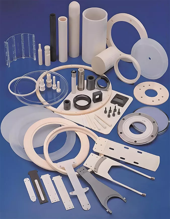
As semiconductor manufacturing advances toward smaller process nodes, higher integration density, and ultra-clean production environments, precision ceramic components have become indispensable throughout semiconductor fabrication equipment. Advanced ceramics are widely used in lithography, etching, thin-film deposition, ion implantation, CMP, packaging, and wafer handling systems. These ceramic components serve critical functions including wafer support, plasma resistance, insulation, gas distribution, thermal management, contamination control, and precision motion guidance. Due to their exceptional hardness, thermal stability, corrosion resistance, low particle generation, and electrical properties, precision ceramics have become key enabling materials for next-generation semiconductor manufacturing. Why Precision Ceramics Matter in Semiconductor Equipment Modern semiconductor equipment operates under extremely demanding conditions: Traditional metallic materials often

半導体装置用精密セラミック部品:先進セラミック・アプリケーションの包括的概要 続きを読む »

半導体製造における先進セラミック材料:高純度、高耐熱性、超硬度性能

As semiconductor technology continues to evolve toward smaller nodes, higher integration density, and more complex manufacturing processes, the demand for advanced materials inside semiconductor equipment has increased dramatically. Modern semiconductor fabrication environments require materials capable of withstanding extreme temperatures, corrosive plasma exposure, ultra-clean vacuum conditions, and high mechanical stress while maintaining dimensional stability and contamination control. Among the many material solutions available today, advanced ceramics have become indispensable in semiconductor manufacturing equipment due to their exceptional combination of mechanical, thermal, electrical, and chemical properties. From wafer handling systems and etching chambers to deposition equipment and thermal processing furnaces, advanced ceramic components are widely used throughout the semiconductor production chain. Why

半導体製造における先進セラミック材料:高純度、高耐熱性、超硬度性能 続きを読む »

半導体製造における先進セラミック部品:静電チャックの原理と動向

1. Introduction: Role of Advanced Ceramics in Semiconductor Equipment In modern semiconductor manufacturing, equipment operates under extreme conditions such as vacuum environments, high temperatures, plasma exposure, and ultra-precision motion control. Traditional metallic materials often fail to meet the combined requirements of stability, cleanliness, electrical insulation, and thermal management. Advanced engineering ceramics—such as alumina (Al₂O₃), aluminum nitride (AlN), and silicon carbide (SiC)—have therefore become essential materials for critical semiconductor components. After precision forming and ultra-precision machining, these ceramics are widely used in key process equipment including lithography, etching, thin-film deposition, ion implantation, and chemical mechanical planarization (CMP). Among these components, the electrostatic chuck (ESC) represents one of the most important functional

半導体製造における先進セラミック部品:静電チャックの原理と動向 続きを読む »