テクニカル・インサイト

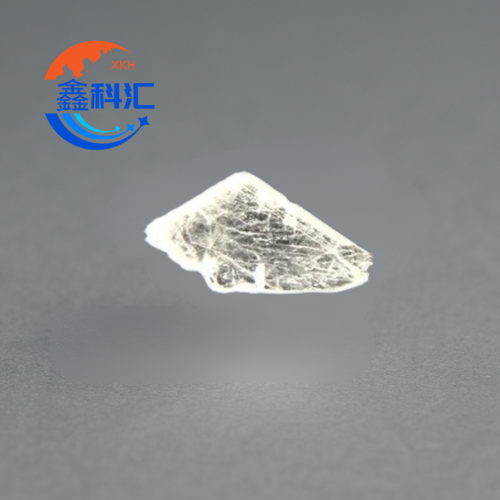
デバイスグレードのhBN単結晶とは何か、そしてなぜそれが先端エレクトロニクスにとって重要なのか?

As the fields of two-dimensional (2D) materials, quantum devices, and next-generation semiconductors continue to evolve, one material has emerged as a critical foundation for many of the most promising technological breakthroughs: Device-Grade Hexagonal Boron Nitride (hBN) Single Crystal. Often referred to as the “ideal companion” to graphene, high-quality hBN has become indispensable in the fabrication of advanced electronic, photonic, and quantum devices. Researchers around the world rely on device-grade hBN to achieve higher carrier mobility, improved device stability, and unprecedented levels of performance in nanoscale systems. But what exactly is device-grade hBN single crystal, and why has it become so important in modern electronics? Understanding Hexagonal Boron Nitride Hexagonal Boron […]

デバイスグレードのhBN単結晶とは何か、そしてなぜそれが先端エレクトロニクスにとって重要なのか? 続きを読む »
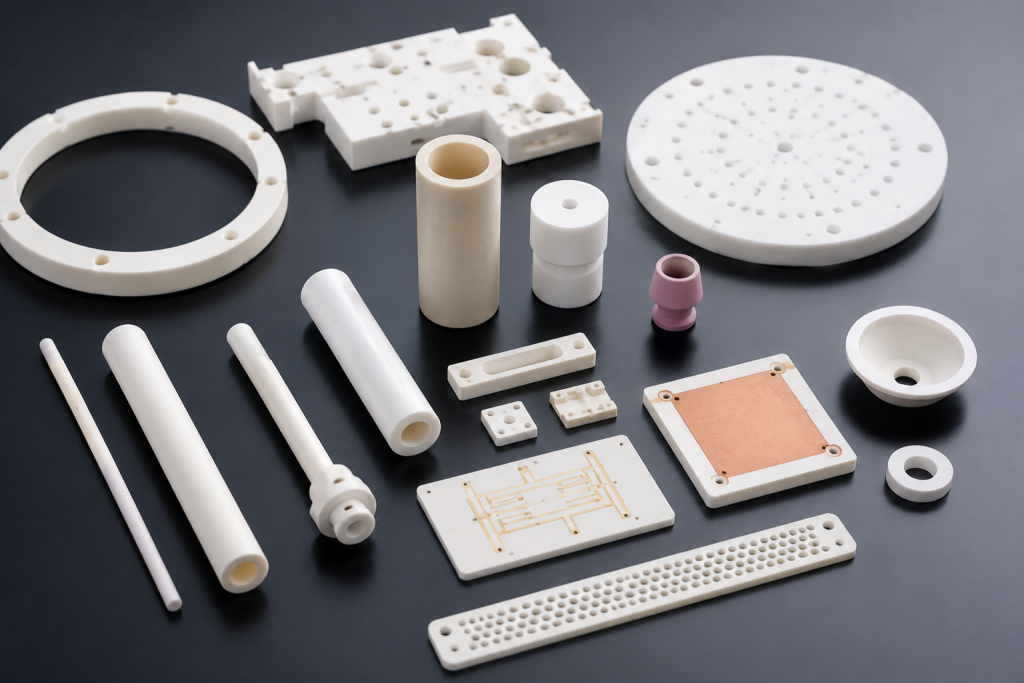
半導体用セラミックス:現代のエレクトロニクスを支える先端材料

As semiconductor devices continue to become smaller, faster, and more powerful, the materials used in semiconductor manufacturing equipment must meet increasingly demanding performance requirements. Traditional metals and polymers often struggle to withstand extreme temperatures, corrosive chemicals, plasma environments, and ultra-clean processing conditions. This is where semiconductor ceramics play a critical role. Advanced ceramic materials combine exceptional thermal stability, electrical insulation, mechanical strength, wear resistance, and chemical durability, making them indispensable in semiconductor fabrication, power electronics, and advanced packaging technologies. Today, semiconductor ceramics are widely used in wafer processing equipment, plasma chambers, vacuum systems, electronic substrates, sensors, and next-generation power devices. What Are Semiconductor Ceramics? Semiconductor ceramics belong to a broader

半導体用セラミックス:現代のエレクトロニクスを支える先端材料 続きを読む »

炭化ケイ素セラミックが優れた耐摩耗性と耐食性を提供する理由

Advanced ceramic materials have become increasingly important in industries that demand exceptional durability, chemical stability, and long service life. Among these materials, silicon carbide (SiC) ceramics have gained widespread recognition for their outstanding wear resistance and corrosion resistance. As a result, silicon carbide components are widely used in semiconductor manufacturing, chemical processing, energy production, mining, aerospace, and mechanical engineering. The superior performance of silicon carbide ceramics is not merely the result of high hardness. Instead, it arises from a unique combination of crystal structure, strong atomic bonding, low porosity, and excellent chemical inertness. Understanding these characteristics helps explain why silicon carbide remains one of the most reliable engineering materials in

炭化ケイ素セラミックが優れた耐摩耗性と耐食性を提供する理由 続きを読む »

なぜアドバンスト・セラミックスはエレクトロニクスで重要なのか?特性、用途、利点

The electronics industry is evolving toward higher power density, smaller device sizes, and more demanding operating environments. From semiconductor fabrication to power electronics and precision sensors, materials are expected to deliver stability under heat, prevent electrical interference, and maintain dimensional accuracy over long service periods. This is where advanced ceramics play a critical role. Materials such as alumina, zirconia, silicon carbide, and aluminum nitride have become essential in modern electronic systems due to their unique combination of electrical, thermal, and mechanical properties. What Are Advanced Ceramics? Advanced ceramics (also called technical ceramics or engineering ceramics) are high-performance inorganic materials engineered for demanding industrial applications. Unlike traditional ceramics used in pottery

なぜアドバンスト・セラミックスはエレクトロニクスで重要なのか?特性、用途、利点 続きを読む »

アドバンスト・セラミックスはいかにして半導体装置の性能を向上させるか

The semiconductor industry operates at the limits of precision engineering. Modern fabrication processes require extreme temperatures, highly reactive chemicals, plasma exposure, vacuum environments, and contamination control at microscopic scales. As integrated circuits continue advancing toward smaller process nodes and larger wafer sizes, equipment performance requirements become increasingly demanding. Under these conditions, material selection becomes a critical factor influencing manufacturing yield, process stability, and equipment lifetime. Traditional metallic materials often struggle to satisfy the severe environmental requirements found inside semiconductor systems. Consequently, advanced ceramics have emerged as indispensable materials in semiconductor equipment. Through their exceptional thermal stability, chemical resistance, mechanical strength, and low contamination characteristics, advanced ceramics significantly improve the performance

アドバンスト・セラミックスはいかにして半導体装置の性能を向上させるか 続きを読む »