기술 인사이트

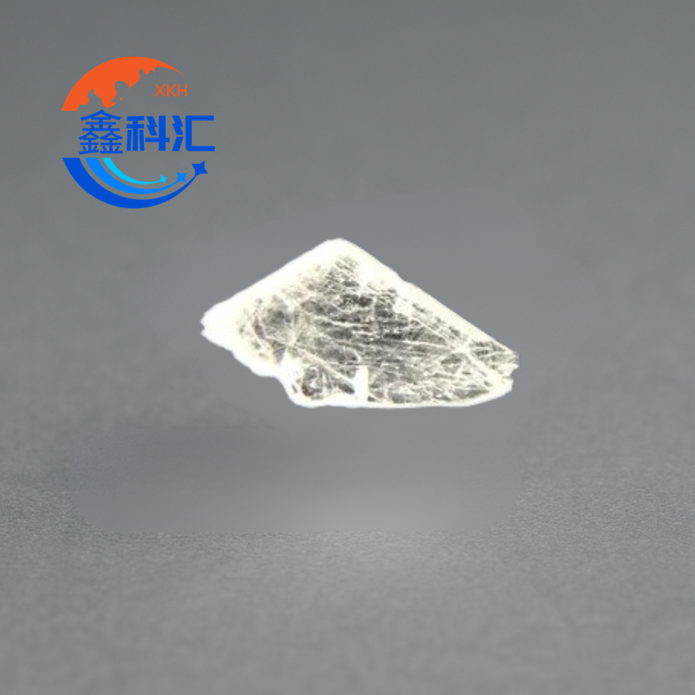
디바이스 등급 hBN 단결정이란 무엇이며, 왜 첨단 전자 산업에서 중요한가?

As the fields of two-dimensional (2D) materials, quantum devices, and next-generation semiconductors continue to evolve, one material has emerged as a critical foundation for many of the most promising technological breakthroughs: Device-Grade Hexagonal Boron Nitride (hBN) Single Crystal. Often referred to as the “ideal companion” to graphene, high-quality hBN has become indispensable in the fabrication […]

디바이스 등급 hBN 단결정이란 무엇이며, 왜 첨단 전자 산업에서 중요한가? 더 읽기"

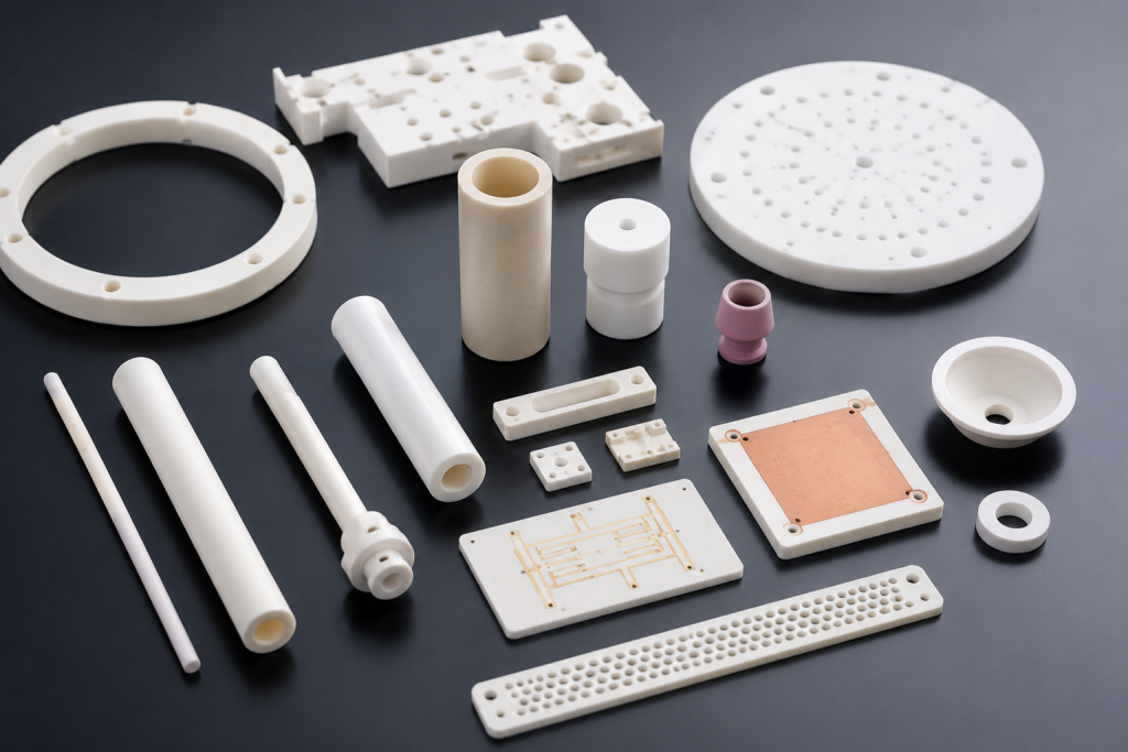
반도체 세라믹: 현대 전자기기를 이끄는 첨단 소재

As semiconductor devices continue to become smaller, faster, and more powerful, the materials used in semiconductor manufacturing equipment must meet increasingly demanding performance requirements. Traditional metals and polymers often struggle to withstand extreme temperatures, corrosive chemicals, plasma environments, and ultra-clean processing conditions. This is where semiconductor ceramics play a critical role. Advanced ceramic materials combine

반도체 세라믹: 현대 전자기기를 이끄는 첨단 소재 더 읽기"

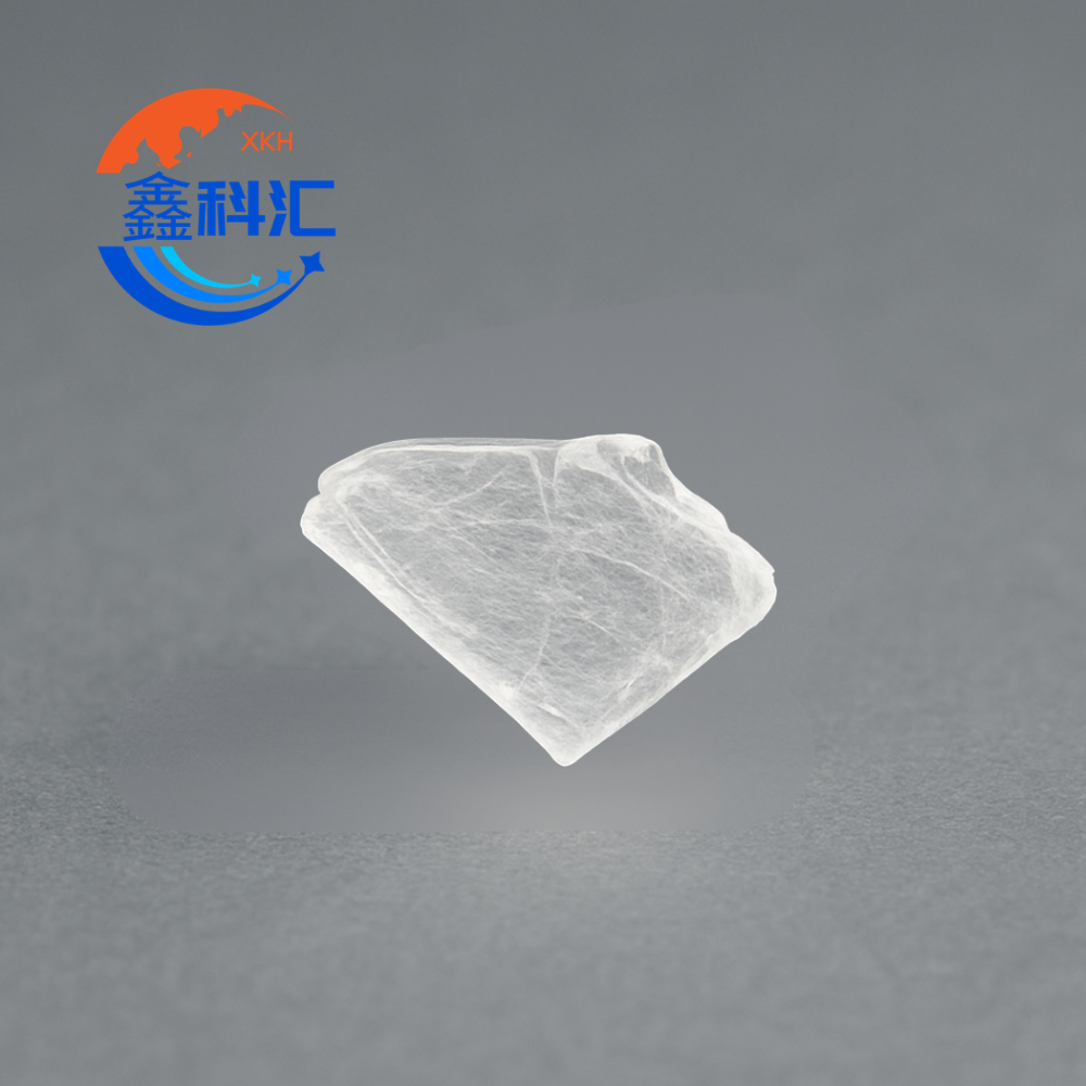
실리콘 카바이드 세라믹이 우수한 내마모성과 내식성을 제공하는 이유

Advanced ceramic materials have become increasingly important in industries that demand exceptional durability, chemical stability, and long service life. Among these materials, silicon carbide (SiC) ceramics have gained widespread recognition for their outstanding wear resistance and corrosion resistance. As a result, silicon carbide components are widely used in semiconductor manufacturing, chemical processing, energy production, mining,

실리콘 카바이드 세라믹이 우수한 내마모성과 내식성을 제공하는 이유 더 읽기"

첨단 세라믹이 전자제품에 중요한 이유는 무엇일까요? 특성, 응용 분야 및 이점

The electronics industry is evolving toward higher power density, smaller device sizes, and more demanding operating environments. From semiconductor fabrication to power electronics and precision sensors, materials are expected to deliver stability under heat, prevent electrical interference, and maintain dimensional accuracy over long service periods. This is where advanced ceramics play a critical role. Materials

첨단 세라믹이 전자제품에 중요한 이유는 무엇일까요? 특성, 응용 분야 및 이점 더 읽기"

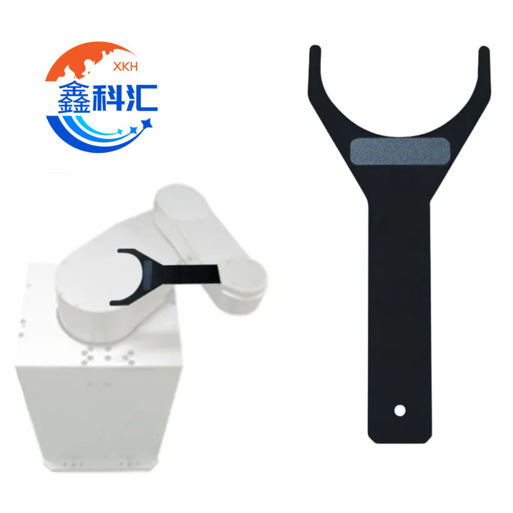
첨단 세라믹이 반도체 장비 성능을 향상시키는 방법

The semiconductor industry operates at the limits of precision engineering. Modern fabrication processes require extreme temperatures, highly reactive chemicals, plasma exposure, vacuum environments, and contamination control at microscopic scales. As integrated circuits continue advancing toward smaller process nodes and larger wafer sizes, equipment performance requirements become increasingly demanding. Under these conditions, material selection becomes a

첨단 세라믹이 반도체 장비 성능을 향상시키는 방법 더 읽기"