Technické poznatky

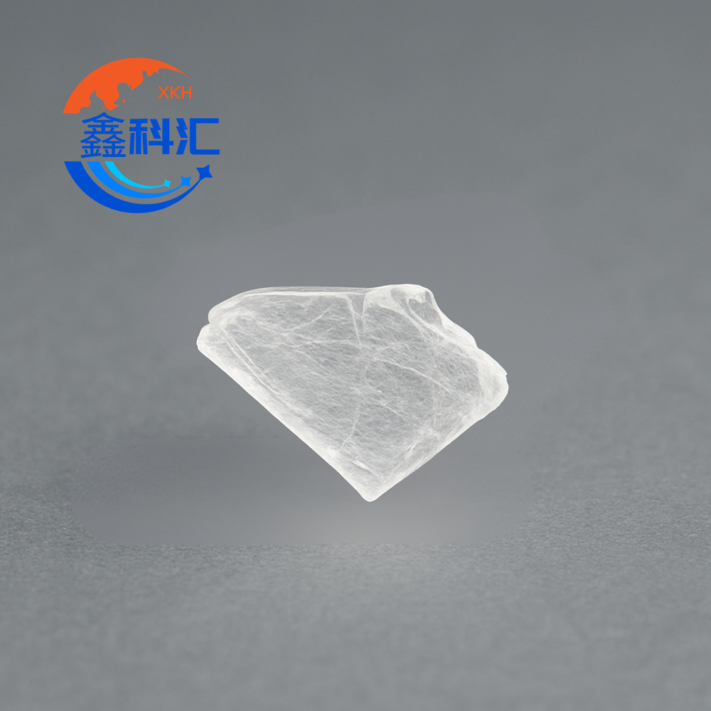
Proč zařízení s vysoce mobilním grafenem závisí na monokrystalech hBN

Graphene is widely regarded as one of the most remarkable materials ever discovered. Its exceptional electrical conductivity, mechanical strength, and atomic thickness have opened new possibilities in nanoelectronics, sensing, and quantum technologies. However, one of the most important discoveries in graphene research is that its performance is not solely determined by graphene itself—but critically depends […]

Proč zařízení s vysoce mobilním grafenem závisí na monokrystalech hBN Číst více »
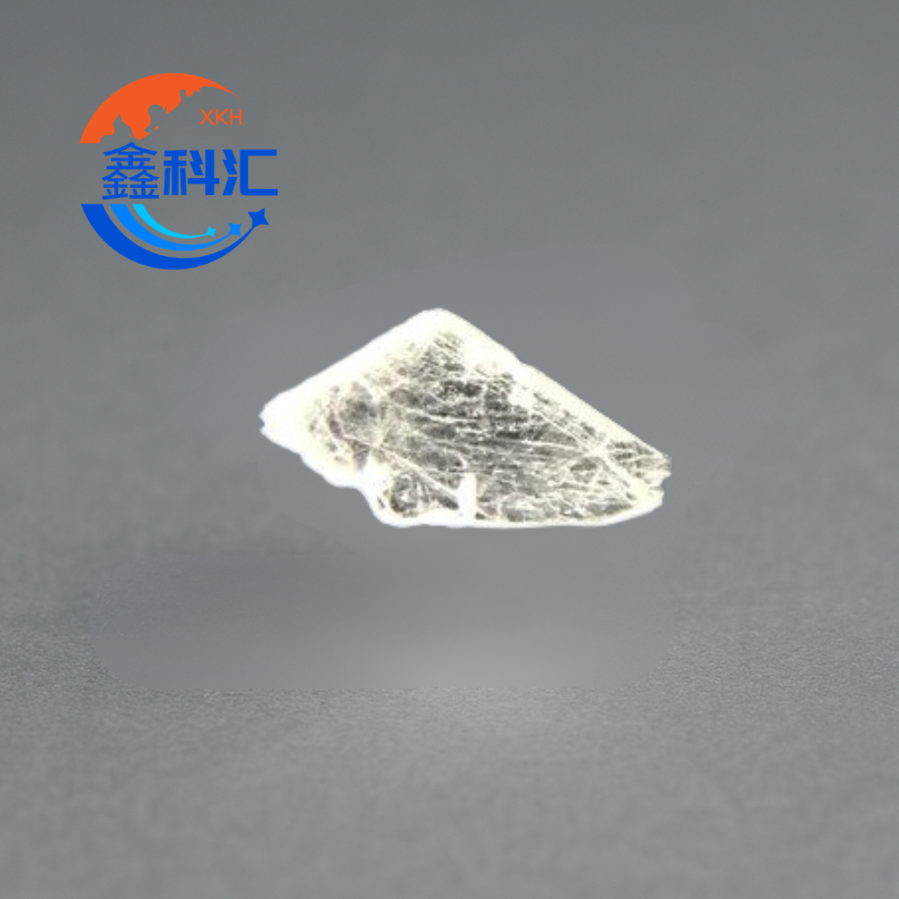
Co je to monokrystal hBN v kvalitě pro elektronická zařízení a proč je důležitý pro pokročilou elektroniku?

As the fields of two-dimensional (2D) materials, quantum devices, and next-generation semiconductors continue to evolve, one material has emerged as a critical foundation for many of the most promising technological breakthroughs: Device-Grade Hexagonal Boron Nitride (hBN) Single Crystal. Often referred to as the “ideal companion” to graphene, high-quality hBN has become indispensable in the fabrication

Co je to monokrystal hBN v kvalitě pro elektronická zařízení a proč je důležitý pro pokročilou elektroniku? Číst více »

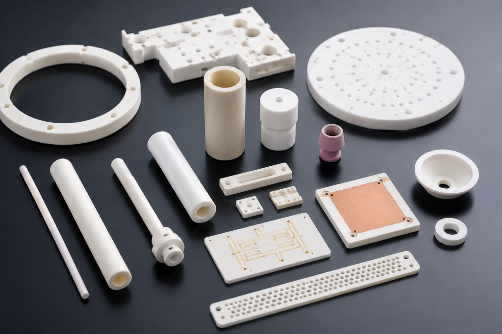
Polovodičová keramika: Pokročilé materiály pohánějící moderní elektroniku

As semiconductor devices continue to become smaller, faster, and more powerful, the materials used in semiconductor manufacturing equipment must meet increasingly demanding performance requirements. Traditional metals and polymers often struggle to withstand extreme temperatures, corrosive chemicals, plasma environments, and ultra-clean processing conditions. This is where semiconductor ceramics play a critical role. Advanced ceramic materials combine

Polovodičová keramika: Pokročilé materiály pohánějící moderní elektroniku Číst více »

Proč je keramika z karbidu křemíku mimořádně odolná proti opotřebení a korozi?

Advanced ceramic materials have become increasingly important in industries that demand exceptional durability, chemical stability, and long service life. Among these materials, silicon carbide (SiC) ceramics have gained widespread recognition for their outstanding wear resistance and corrosion resistance. As a result, silicon carbide components are widely used in semiconductor manufacturing, chemical processing, energy production, mining,

Proč je keramika z karbidu křemíku mimořádně odolná proti opotřebení a korozi? Číst více »

Proč je pokročilá keramika v elektronice důležitá? Vlastnosti, aplikace a přínosy

The electronics industry is evolving toward higher power density, smaller device sizes, and more demanding operating environments. From semiconductor fabrication to power electronics and precision sensors, materials are expected to deliver stability under heat, prevent electrical interference, and maintain dimensional accuracy over long service periods. This is where advanced ceramics play a critical role. Materials

Proč je pokročilá keramika v elektronice důležitá? Vlastnosti, aplikace a přínosy Číst více »

Jak pokročilá keramika zlepšuje výkon polovodičových zařízení

The semiconductor industry operates at the limits of precision engineering. Modern fabrication processes require extreme temperatures, highly reactive chemicals, plasma exposure, vacuum environments, and contamination control at microscopic scales. As integrated circuits continue advancing toward smaller process nodes and larger wafer sizes, equipment performance requirements become increasingly demanding. Under these conditions, material selection becomes a

Jak pokročilá keramika zlepšuje výkon polovodičových zařízení Číst více »