技術洞察

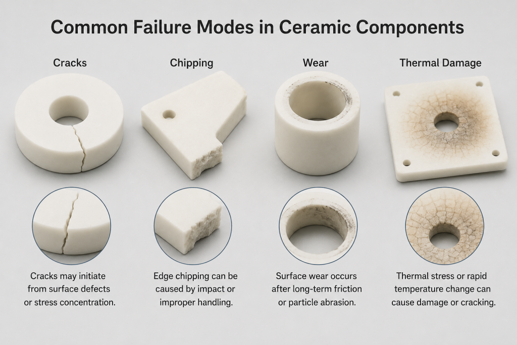
Ceramic Components Failure Analysis: Cracks, Chipping, Wear and Thermal Damage

Advanced ceramic components are widely used in semiconductor equipment, vacuum systems, precision machinery, electrical insulation, chemical processing and high-temperature applications. Materials such as alumina, zirconia, aluminum nitride, silicon carbide and silicon nitride provide excellent hardness, wear resistance, corrosion resistance, electrical insulation and dimensional stability. Despite these advantages, ceramic components can still fail. Unlike most metals, […]

Ceramic Components Failure Analysis: Cracks, Chipping, Wear and Thermal Damage 閱讀更多 »

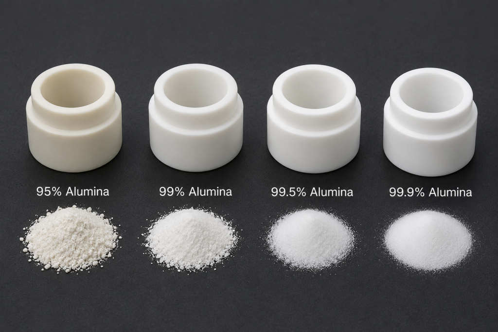
Alumina Ceramic Purity Levels Explained: 95%, 99%, 99.5% and 99.9% Compared

Alumina ceramic, also known as aluminum oxide ceramic or Al₂O₃ ceramic, is one of the most widely used technical ceramic materials. It offers a practical combination of electrical insulation, mechanical strength, hardness, wear resistance, thermal stability and corrosion resistance. However, not all alumina ceramics are the same. Commercial alumina materials are commonly identified by their

Alumina Ceramic Purity Levels Explained: 95%, 99%, 99.5% and 99.9% Compared 閱讀更多 »

Structural Ceramics for Semiconductor Manufacturing: Key Materials and Equipment Applications

Semiconductor manufacturing requires materials that can operate reliably under high temperature, plasma exposure, chemical corrosion, vacuum conditions and strict cleanliness requirements. In many process tools, metal and plastic components cannot meet these demanding conditions. This is why structural ceramics are widely used in semiconductor equipment. Structural ceramics are advanced ceramic materials designed to provide mechanical

Structural Ceramics for Semiconductor Manufacturing: Key Materials and Equipment Applications 閱讀更多 »

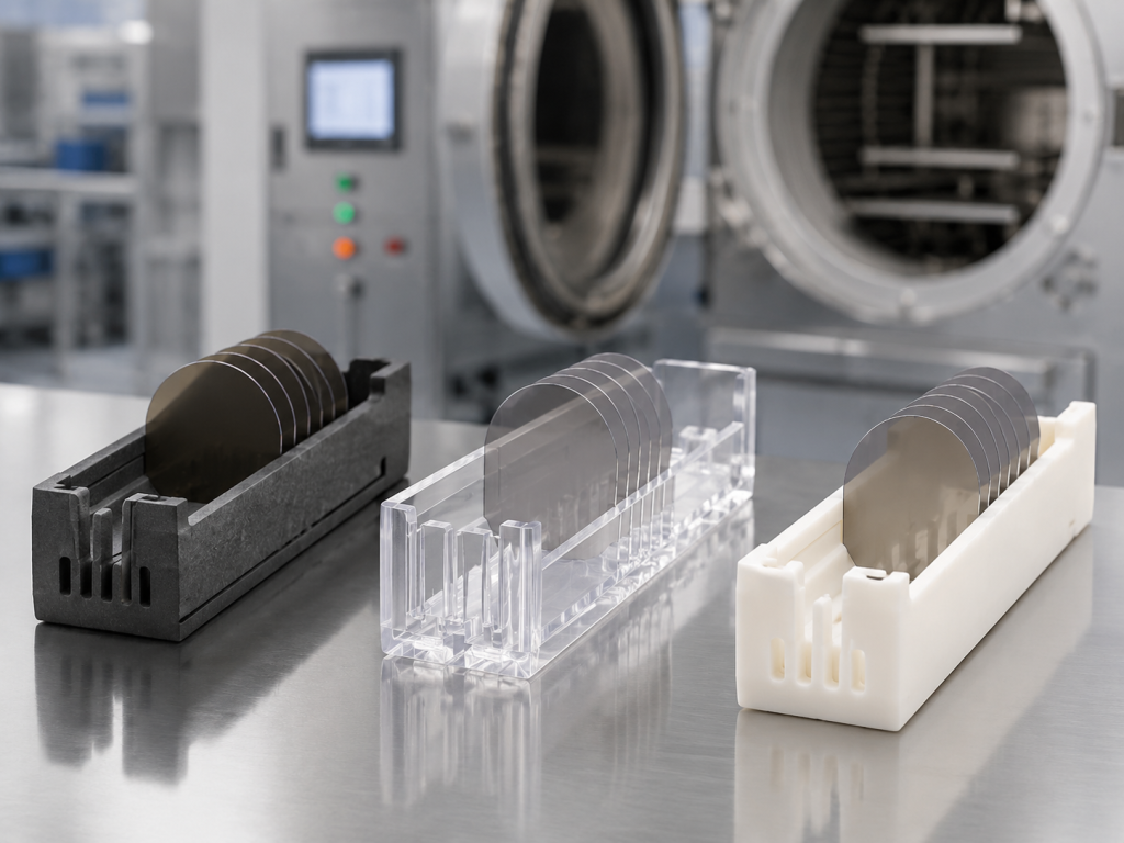
Semiconductor Wafer Boat Materials: SiC, Quartz and Alumina Compared

In semiconductor manufacturing, wafer boats are used to hold and support wafers during high-temperature processes such as diffusion, oxidation, annealing and LPCVD. Although the structure of a wafer boat may look simple, the material choice is very important. Different materials can affect thermal stability, contamination control, mechanical strength, service life and overall process reliability. Among

Semiconductor Wafer Boat Materials: SiC, Quartz and Alumina Compared 閱讀更多 »

What Is a Semiconductor Wafer Boat? Materials, Structure and Applications

In semiconductor manufacturing, wafers must be processed, transported, heated and cooled under highly controlled conditions. During high-temperature processes such as diffusion, oxidation, annealing and LPCVD, wafers cannot simply be placed directly inside a furnace. They need a stable, clean and precisely designed carrier to hold them in position. This carrier is commonly known as a

What Is a Semiconductor Wafer Boat? Materials, Structure and Applications 閱讀更多 »

Overcoming the Challenges of Manufacturing Complex Semiconductor Ceramic Components

Advanced ceramics have become indispensable materials in modern semiconductor equipment. Components used in plasma etching, chemical vapor deposition (CVD), physical vapor deposition (PVD), ion implantation, and wafer handling systems must operate reliably under extreme conditions, including high-energy plasma exposure, corrosive process gases, elevated temperatures, thermal cycling, and high-voltage electrical fields. Materials such as alumina (Al₂O₃),

Overcoming the Challenges of Manufacturing Complex Semiconductor Ceramic Components 閱讀更多 »

多孔碳化矽(SiC)陶瓷支撐體:低溫燒結技術與性能研究

Silicon Carbide (SiC) porous ceramic supports are widely used in advanced membrane filtration systems due to their excellent thermal stability, high mechanical strength, and superior chemical resistance. SiC-based ceramic materials are especially suitable for harsh environments such as high-temperature filtration, wastewater treatment, and chemical processing. However, conventional SiC ceramics require extremely high sintering temperatures (>2000°C),

多孔碳化矽(SiC)陶瓷支撐體:低溫燒結技術與性能研究 閱讀更多 »

碳化矽陶瓷:適用於極端工業環境的先進工程材料

As industrial equipment continues to evolve toward higher precision, higher temperatures, and more demanding operating conditions, conventional materials such as metals and standard ceramics are increasingly reaching their performance limits. Wear, thermal deformation, chemical corrosion, particle contamination, and electrical instability can all negatively impact manufacturing efficiency, product quality, and equipment lifespan. Among advanced engineering materials,

碳化矽陶瓷:適用於極端工業環境的先進工程材料 閱讀更多 »

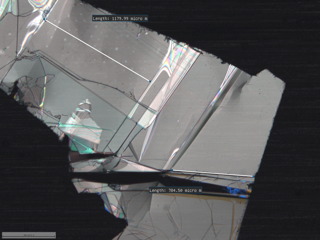
hBN 如何推動次世代二維材料的發展

The rapid expansion of two-dimensional (2D) materials research has opened entirely new directions in electronics, photonics, and quantum technologies. Materials such as graphene, transition metal dichalcogenides (TMDs), and other atomically thin crystals exhibit extraordinary properties that differ fundamentally from their bulk counterparts. However, the practical realization of high-performance 2D devices depends not only on the

hBN 如何推動次世代二維材料的發展 閱讀更多 »

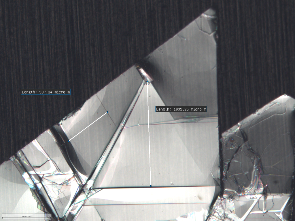
為何裝置級 hBN 正成為未來半導體的戰略性材料

As semiconductor technology continues to scale beyond traditional silicon-based architectures, the industry is increasingly turning toward new classes of materials that can support higher performance, lower power consumption, and fundamentally new device physics. Among these emerging materials, device-grade hexagonal boron nitride (hBN) single crystal has rapidly gained attention as a strategic enabler for next-generation electronics.

為何裝置級 hBN 正成為未來半導體的戰略性材料 閱讀更多 »

為何高遷移率石墨烯元件依賴 hBN 單晶

Graphene is widely regarded as one of the most remarkable materials ever discovered. Its exceptional electrical conductivity, mechanical strength, and atomic thickness have opened new possibilities in nanoelectronics, sensing, and quantum technologies. However, one of the most important discoveries in graphene research is that its performance is not solely determined by graphene itself—but critically depends

為何高遷移率石墨烯元件依賴 hBN 單晶 閱讀更多 »