Wiadomości branżowe

Ceramiczny uchwyt próżniowy

Porowata ceramika w produkcji półprzewodników: Precyzja dzięki zaawansowanemu projektowaniu materiałów

Porous ceramics are engineered ceramic materials produced through specialized processing techniques that create interconnected or closed pore structures within the material. Their porosity typically ranges from 20% to 90%, while pore sizes can vary from nanometer scale to millimeter scale depending on design requirements. Thanks to their unique internal architecture and outstanding physical properties—including high-temperature […]
Porowata ceramika w produkcji półprzewodników: Precyzja dzięki zaawansowanemu projektowaniu materiałów Dowiedz się więcej »

Ceramika półprzewodnikowa wyjaśniona: Funkcjonalna ceramika elektroniczna przekształcająca nowoczesną technologię

Semiconductor ceramics are a specialized class of electronic ceramic materials engineered to exhibit semiconductor behavior through controlled material modification. Unlike traditional conductive materials, their electrical properties are highly sensitive to external conditions such as temperature, light, electric fields, humidity, and surrounding gases. This unique responsiveness allows semiconductor ceramics to convert environmental changes into electrical signals,

Ceramika półprzewodnikowa wyjaśniona: Funkcjonalna ceramika elektroniczna przekształcająca nowoczesną technologię Dowiedz się więcej »

Podłoża ceramiczne: Podstawowa rewolucja materiałowa napędzająca obliczenia AI, moduły optyczne i półprzewodniki mocy

As artificial intelligence computing accelerates, data transmission speeds increase, and next-generation power electronics continue to evolve, semiconductor packaging technologies are undergoing a fundamental transformation. Conventional substrate materials are increasingly facing limitations in thermal management, electrical performance, and integration density. Against this backdrop, ceramic substrates are emerging from niche applications to become critical enabling materials for

Podłoża ceramiczne: Podstawowa rewolucja materiałowa napędzająca obliczenia AI, moduły optyczne i półprzewodniki mocy Dowiedz się więcej »

Komponenty ceramiczne z tlenku glinu w sprzęcie półprzewodnikowym: Funkcje, struktury i zaawansowane zastosowania

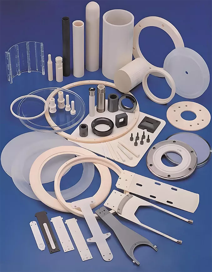
As semiconductor devices continue evolving toward smaller nodes, higher integration density, and greater processing precision, the demand for ultra-clean, heat-resistant, and plasma-stable materials inside semiconductor equipment has increased significantly. Among advanced engineering ceramics, high-purity alumina ceramic (Al₂O₃) remains one of the most widely used materials across semiconductor manufacturing systems. From plasma etching chambers to wafer

Komponenty ceramiczne z tlenku glinu w sprzęcie półprzewodnikowym: Funkcje, struktury i zaawansowane zastosowania Dowiedz się więcej »

Precyzyjne komponenty ceramiczne do urządzeń półprzewodnikowych: Kompleksowy przegląd zaawansowanych zastosowań ceramiki

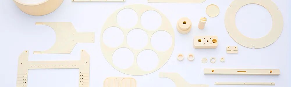
As semiconductor manufacturing advances toward smaller process nodes, higher integration density, and ultra-clean production environments, precision ceramic components have become indispensable throughout semiconductor fabrication equipment. Advanced ceramics are widely used in lithography, etching, thin-film deposition, ion implantation, CMP, packaging, and wafer handling systems. These ceramic components serve critical functions including wafer support, plasma resistance, insulation,

Precyzyjne komponenty ceramiczne do urządzeń półprzewodnikowych: Kompleksowy przegląd zaawansowanych zastosowań ceramiki Dowiedz się więcej »

Zaawansowane materiały ceramiczne w produkcji półprzewodników: Wysoka czystość, ekstremalna odporność na ciepło i bardzo wysoka wydajność

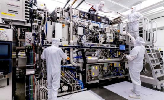
As semiconductor technology continues to evolve toward smaller nodes, higher integration density, and more complex manufacturing processes, the demand for advanced materials inside semiconductor equipment has increased dramatically. Modern semiconductor fabrication environments require materials capable of withstanding extreme temperatures, corrosive plasma exposure, ultra-clean vacuum conditions, and high mechanical stress while maintaining dimensional stability and contamination

Zaawansowane materiały ceramiczne w produkcji półprzewodników: Wysoka czystość, ekstremalna odporność na ciepło i bardzo wysoka wydajność Dowiedz się więcej »

Zaawansowane komponenty ceramiczne w produkcji półprzewodników: Zasady i trendy dotyczące uchwytów elektrostatycznych

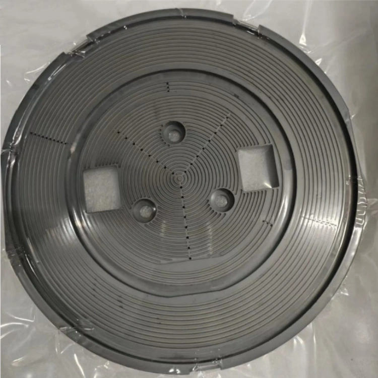
1. Introduction: Role of Advanced Ceramics in Semiconductor Equipment In modern semiconductor manufacturing, equipment operates under extreme conditions such as vacuum environments, high temperatures, plasma exposure, and ultra-precision motion control. Traditional metallic materials often fail to meet the combined requirements of stability, cleanliness, electrical insulation, and thermal management. Advanced engineering ceramics—such as alumina (Al₂O₃), aluminum

Zaawansowane komponenty ceramiczne w produkcji półprzewodników: Zasady i trendy dotyczące uchwytów elektrostatycznych Dowiedz się więcej »