


 Al₂O₃ 氧化鋁陶瓷基板是電子、半導體加工和工業應用中使用最廣泛的先進陶瓷材料之一。氧化鋁陶瓷基板具有優異的電絕緣性、高機械強度、強耐腐蝕性和穩定的熱性,為要求在嚴苛操作條件下仍能保持可靠性的應用提供了理想的解決方案。.
這些基板由 96% 至 99.6% 的高純度氧化鋁陶瓷材料製成,使用精密的陶瓷成型和拋光製程生產,以確保卓越的平面度、致密的結構和優異的表面品質。與許多工程材料相比,氧化鋁陶瓷兼具效能與成本效益,是厚膜電路、LED 散熱、電源模組及半導體設備元件的首選。.
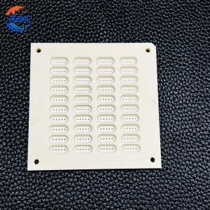
可根據客戶要求提供客製尺寸、表面精加工和機械加工服務。.
產品規格
| 參數 | 規格 |
|---|---|
| 產品名稱 | Al₂O₃ 氧化鋁陶瓷基板 |
| 材質 | 高純度氧化鋁陶瓷 |
| 純淨 | 96%、99%、99.6% 選購品 |
| 顏色 | 白色/象牙色 |
| 厚度 | 0.385-2.5 mm 或客製化 |
| 表面類型 | 單面或雙面拋光 |
| 標準表面粗度 | Ra 0.8-1.0 μm |
| 精細拋光 | Ra < 5 奈米 |
| 鑽石鏡面上光 | Ra < 1 奈米 |
| 吸水率 | 0% |
| 最高操作溫度 | 高達 1700°C |
| 體積電阻率 | >10¹⁴ Ω-cm |
| 包裝 | 卡式帶盒或客製化 |
| 客製化服務 | 機械加工、金屬化、表面處理 |
典型材料特性
| 屬性 | Al₂O₃ 96% | Al₂O₃ 99% | Al₂O₃ 99.6% |
|---|---|---|---|
| 密度 (g/cm³) | 3.7 | 3.9 | 3.9 |
| Vickers Hardness (GPa) | 11.5 | 13 | 14 |
| 抗彎強度 (MPa) | 358 | 380 | 380 |
| Compressive Strength (MPa) | 2300 | 3000 | 3000 |
| 熱傳導率 (W/m-K) | 24–25 | 25–30 | 25-35 |
| Thermal Shock Resistance (ΔT°C) | 250 | 200 | 200 |
| 體積電阻率 (Ω-cm) | >10¹⁴ | >10¹⁴ | >10¹⁴ |
主要功能
絕佳的電氣絕緣性
Alumina ceramic exhibits high dielectric strength and electrical resistivity, providing stable insulation performance in electronic and semiconductor systems.
高機械強度
With excellent hardness and compressive strength, alumina ceramic substrates maintain dimensional stability and long service life under demanding operating environments.
優異的耐腐蝕性
Al₂O₃ ceramic demonstrates strong resistance to acids, alkalis, and many chemical media, making it suitable for chemically aggressive industrial environments.
高溫穩定性
The material maintains excellent structural performance under elevated temperatures and can operate continuously in harsh thermal conditions.
Low Porosity Structure
Dense microstructure minimizes contamination risk and supports high process consistency for precision applications.
優異的耐磨性
The high hardness of alumina ceramic significantly improves durability and extends operational lifetime.
 Surface Finishing Options
Different surface processing methods are available according to application requirements:
Standard Polish
Ra: 0.8–1.0 μm
Fine Polish
Ra: <5 nm
鑽石鏡面上光
Ra: <1 nm
Single-side polishing, double-side polishing, grinding, and special surface treatments can be customized.
 典型應用
典型應用
Al₂O₃ ceramic substrates are widely used in:
- 半導體加工設備
- Thick-film hybrid integrated circuits (HIC)
- Thin-film electronic devices
- LED heat dissipation substrates
- IGBT power modules
- Electronic insulation components
- Capacitors and sensors
- Vacuum electronic devices
- High-temperature industrial equipment
- Petrochemical systems
- Communication engineering equipment
- Precision industrial components
Standard Available Sizes
Various standard and customized dimensions are available.
Square Substrates
- 2″ × 2″
- 3″ × 3″
- 4″ × 4″
- 4.5″ × 4.5″
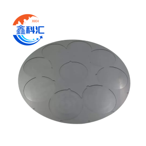
Round Ceramic Wafers
- Multiple standard wafer sizes available
- Thickness options from 0.385 mm to 2.5 mm
- Custom dimensions supported
常見問題
1. What is the difference between Al₂O₃ ceramic substrates and AlN ceramic substrates?
Al₂O₃ and AlN are both commonly used ceramic substrate materials, but they differ in performance characteristics. Alumina offers excellent insulation, corrosion resistance, mechanical strength, and cost efficiency. Aluminum nitride provides significantly higher thermal conductivity and is often selected for high-power heat management applications. Alumina remains one of the most cost-effective choices for general electronic and semiconductor applications.
2. Can alumina ceramic substrates be customized?
Yes. We support customized production according to customer drawings and technical requirements. Available options include:
- Customized thickness
- 精密孔和槽
- Special geometries
- Single or double-side polishing
- Laser machining
- Metallization services
- Semiconductor-grade surface processing
OEM and small-batch production are supported.
3. Why are alumina ceramic substrates widely used in semiconductor industries?
Alumina ceramic substrates combine high electrical insulation, excellent chemical stability, strong mechanical properties, and reliable thermal performance. Their dense structure and smooth surface also help reduce contamination risks and improve process stability. These advantages make them widely used in semiconductor equipment, power electronics, LED packaging, and industrial electronic systems.
為何選擇我們
- 高純度原料
- Strict quality control process
- 精密加工能力
- Stable dimensional tolerance
- Fast production lead time
- OEM and custom design support
- Technical assistance from engineering team
We accept customized drawings and provide tailored ceramic solutions according to your project requirements.
商品評價
目前沒有評價。