


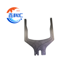
 The Silicon Carbide (SiC) Ceramic End Effector is a high-precision wafer handling component designed for semiconductor automation systems, including wafer transfer robots, AMHS systems, EUV lithography equipment, and high-temperature process tools.
Made from high-purity CVD SiC or engineered SSiC, this end effector delivers exceptional rigidity, ultra-low particle generation, and outstanding thermal and chemical stability. It is widely used in 300mm and advanced node semiconductor fabs, where contamination control and positioning accuracy are critical.
Compared with traditional aluminum or quartz end effectors, SiC ceramic solutions significantly improve process stability, wafer safety, and equipment lifetime.
Key Advantages
Ultra-Low Particle Contamination
- Particle generation: <0.1/cm² (SEMI F57 compliant)
- No metal ion contamination
- Ideal for EUV and advanced node processes
High Rigidity & Precision Stability
- Young’s modulus: ~420 GPa
- Prevents vibration-induced wafer misalignment
- Ensures stable high-speed robotic transfer
Excellent Thermal Stability
- Operating temperature: up to 1600°C (oxidizing)
- Up to 1950°C (inert atmosphere)
- Suitable for extreme semiconductor environments
Superior Chemical & Plasma Resistance
- Resistant to acids, alkalis, and plasma environments
- No corrosion in CVD / PVD / etching chambers
- Stable in SiH₄, NH₃, HCl process gases
Wear-Free & Long Service Life
- Vickers hardness: ~2800 HV
- No particle shedding during long-term operation
- Excellent surface durability (Ra < 0.2 μm)
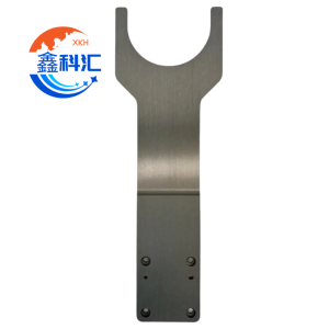
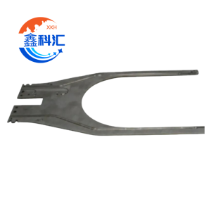
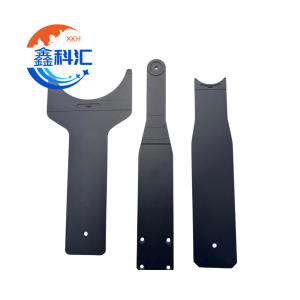
Structural & Design Features
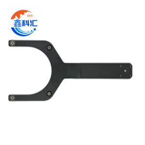
Precision Wafer Handling Geometry
Supports:
- 150mm / 200mm / 300mm / 450mm wafers
- Edge-grip / notch alignment / flat support designs
- Custom robot arm integration
High Stiffness Lightweight Structure
- High rigidity-to-weight ratio
- Suitable for high-speed robotic systems
- Minimizes dynamic deflection during motion
Ultra-Clean Surface Processing
- Precision grinding & polishing
- Low surface roughness
- Cleanroom-compatible structure
Custom Engineering Interface
- Robot arm mounting compatibility
- OEM integration for AMHS systems
- Custom hole positions and fixture design
Material Options
CVD Silicon Carbide (CVD SiC)
- Ultra-high purity
- Best for EUV / advanced semiconductor processes
- Ultra-low contamination level
Sintered Silicon Carbide (SSiC)
- High strength and wear resistance
- Suitable for industrial wafer handling systems
- Excellent cost-performance balance
Technical Specifications
| Item | Specification |
|---|---|
| Material | CVD SiC / SSiC |
| Purity | >99.5% |
| Grain Size | 4–10 μm |
| Density | >3.14 g/cm³ |
| Hardness | ~2800 HV |
| Flexural Strength | 450 MPa |
| Elastic Modulus | 420 GPa |
| Thermal Conductivity | 160 W/m·K |
| Max Temperature | 1600°C (oxidation) / 1950°C (inert) |
| Electrical Resistivity | 10⁶–10⁸ Ω·cm |
| Surface Finish | Ultra-fine polished |
| Size | Custom (150–450mm wafers) |
Applications
Semiconductor Manufacturing
- EUV lithography wafer handling
- 300mm wafer robot transfer systems
- CVD / PVD / etching chamber automation
- Ion implantation wafer transport
Advanced Semiconductor Materials
- SiC power device wafer handling
- GaN epitaxy production systems
- High-temperature MOCVD processes
Photovoltaic & LED Industry
- Solar wafer automation lines
- Micro-LED / Mini-LED transfer systems
- Sapphire wafer handling
Automation & Robotics (AMHS)
- Wafer transport robot arms
- Cleanroom automation systems
- High-speed material handling systems
Research & High-End Equipment
- Quantum device fabrication
- Cryogenic wafer handling systems
- Advanced packaging (3D IC / MEMS)
Product Advantages Summary
- Zero metal contamination risk
- Ultra-high rigidity for precision handling
- Excellent thermal and chemical stability
- Long lifetime with minimal wear
- Compatible with cleanroom automation
- Customizable for all wafer sizes
- Suitable for EUV and advanced nodes
Customization Options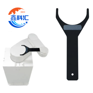
We support full OEM/ODM customization:
- End effector geometry (flat / edge grip / notch align)
- Wafer size compatibility (150–450mm)
- Robot interface design
- Surface coating (anti-static / hydrophobic optional)
- Precision tolerance optimization
- Cleanroom-grade finishing
FAQ
Q1: Why use SiC instead of aluminum or quartz?
- Aluminum: particle generation + oxidation issues
- Quartz: brittle + poor thermal shock resistance
- SiC: best combination of rigidity, cleanliness, and durability
Q2: Can it support 450mm wafers?
Yes, custom designs are available for 450mm wafer handling systems.
Q3: Is it suitable for EUV lithography?
Yes. SiC end effectors meet ultra-low particle and vacuum compatibility requirements.
Q4: Can it be used in vacuum and high-temperature systems?
Yes. SiC performs stably in vacuum, plasma, and high-temperature environments.
Отзывы
Отзывов пока нет.