Información técnica

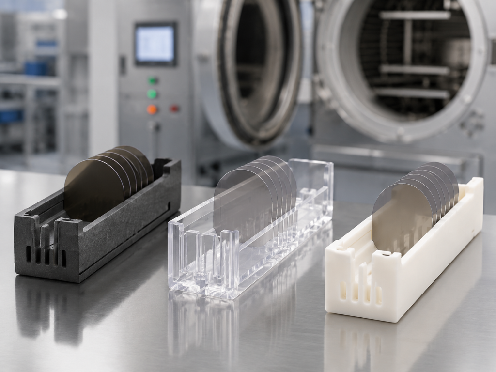
Wafer Boat Slot Geometry Guide: V-Groove, U-Groove, Contact Area and Wafer Edge Protection

Wafer boat performance depends on more than the boat material, wafer capacity and overall dimensions. The geometry of each wafer slot directly affects wafer positioning, edge contact, loading stability, thermal movement and the risk of chipping or particle generation. A slot that is too narrow may grip the wafer edge too tightly. A slot that […]
Wafer Boat Slot Geometry Guide: V-Groove, U-Groove, Contact Area and Wafer Edge Protection Leer más »

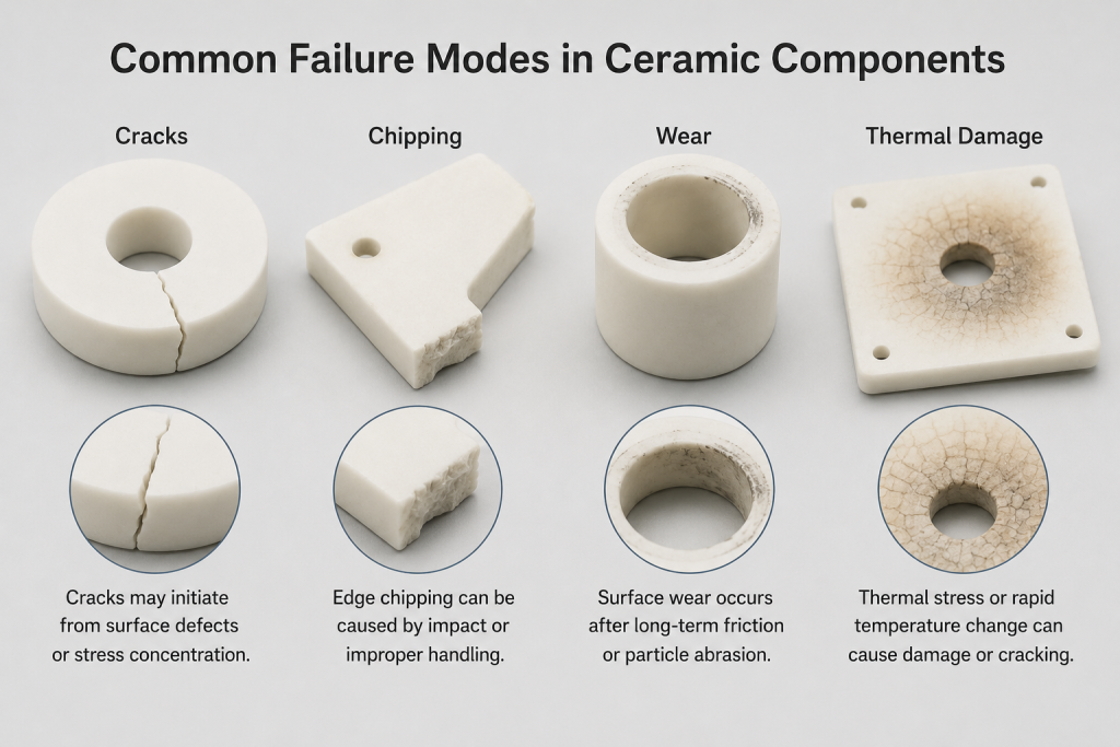
Ceramic Components Failure Analysis: Cracks, Chipping, Wear and Thermal Damage

Advanced ceramic components are widely used in semiconductor equipment, vacuum systems, precision machinery, electrical insulation, chemical processing and high-temperature applications. Materials such as alumina, zirconia, aluminum nitride, silicon carbide and silicon nitride provide excellent hardness, wear resistance, corrosion resistance, electrical insulation and dimensional stability. Despite these advantages, ceramic components can still fail. Unlike most metals,

Ceramic Components Failure Analysis: Cracks, Chipping, Wear and Thermal Damage Leer más »

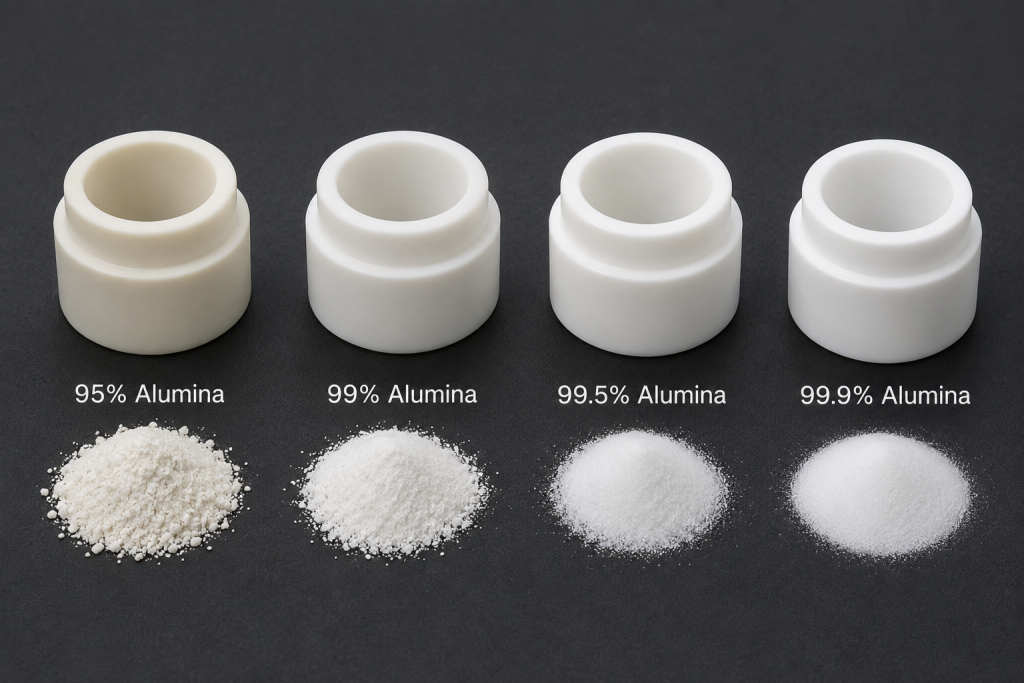
Alumina Ceramic Purity Levels Explained: 95%, 99%, 99.5% and 99.9% Compared

Alumina ceramic, also known as aluminum oxide ceramic or Al₂O₃ ceramic, is one of the most widely used technical ceramic materials. It offers a practical combination of electrical insulation, mechanical strength, hardness, wear resistance, thermal stability and corrosion resistance. However, not all alumina ceramics are the same. Commercial alumina materials are commonly identified by their

Alumina Ceramic Purity Levels Explained: 95%, 99%, 99.5% and 99.9% Compared Leer más »

Structural Ceramics for Semiconductor Manufacturing: Key Materials and Equipment Applications

Semiconductor manufacturing requires materials that can operate reliably under high temperature, plasma exposure, chemical corrosion, vacuum conditions and strict cleanliness requirements. In many process tools, metal and plastic components cannot meet these demanding conditions. This is why structural ceramics are widely used in semiconductor equipment. Structural ceramics are advanced ceramic materials designed to provide mechanical

Structural Ceramics for Semiconductor Manufacturing: Key Materials and Equipment Applications Leer más »

Materiales para soportes de obleas semiconductoras: comparación entre SiC, cuarzo y alúmina

In semiconductor manufacturing, wafer boats are used to hold and support wafers during high-temperature processes such as diffusion, oxidation, annealing and LPCVD. Although the structure of a wafer boat may look simple, the material choice is very important. Different materials can affect thermal stability, contamination control, mechanical strength, service life and overall process reliability. Among

Materiales para soportes de obleas semiconductoras: comparación entre SiC, cuarzo y alúmina Leer más »

¿Qué es una bandeja para obleas semiconductoras? Materiales, estructura y aplicaciones

En la fabricación de semiconductores, las obleas deben procesarse, transportarse, calentarse y enfriarse en condiciones estrictamente controladas. Durante los procesos a alta temperatura, como la difusión, la oxidación, el recocido y el LPCVD, las obleas no pueden colocarse simplemente directamente dentro de un horno. Necesitan un soporte estable, limpio y diseñado con precisión para mantenerlas en su posición. Este soporte se conoce comúnmente como un

¿Qué es una bandeja para obleas semiconductoras? Materiales, estructura y aplicaciones Leer más »

Overcoming the Challenges of Manufacturing Complex Semiconductor Ceramic Components

Advanced ceramics have become indispensable materials in modern semiconductor equipment. Components used in plasma etching, chemical vapor deposition (CVD), physical vapor deposition (PVD), ion implantation, and wafer handling systems must operate reliably under extreme conditions, including high-energy plasma exposure, corrosive process gases, elevated temperatures, thermal cycling, and high-voltage electrical fields. Materials such as alumina (Al₂O₃),

Overcoming the Challenges of Manufacturing Complex Semiconductor Ceramic Components Leer más »

Soporte cerámico de carburo de silicio (SiC) poroso: tecnología de sinterización a baja temperatura y estudio de sus prestaciones

Silicon Carbide (SiC) porous ceramic supports are widely used in advanced membrane filtration systems due to their excellent thermal stability, high mechanical strength, and superior chemical resistance. SiC-based ceramic materials are especially suitable for harsh environments such as high-temperature filtration, wastewater treatment, and chemical processing. However, conventional SiC ceramics require extremely high sintering temperatures (>2000°C),

Soporte cerámico de carburo de silicio (SiC) poroso: tecnología de sinterización a baja temperatura y estudio de sus prestaciones Leer más »

Cerámicas de carburo de silicio: materiales de ingeniería avanzados para entornos industriales extremos

As industrial equipment continues to evolve toward higher precision, higher temperatures, and more demanding operating conditions, conventional materials such as metals and standard ceramics are increasingly reaching their performance limits. Wear, thermal deformation, chemical corrosion, particle contamination, and electrical instability can all negatively impact manufacturing efficiency, product quality, and equipment lifespan. Among advanced engineering materials,

Cerámicas de carburo de silicio: materiales de ingeniería avanzados para entornos industriales extremos Leer más »

Cómo hBN facilita el desarrollo de materiales 2D de última generación

The rapid expansion of two-dimensional (2D) materials research has opened entirely new directions in electronics, photonics, and quantum technologies. Materials such as graphene, transition metal dichalcogenides (TMDs), and other atomically thin crystals exhibit extraordinary properties that differ fundamentally from their bulk counterparts. However, the practical realization of high-performance 2D devices depends not only on the

Cómo hBN facilita el desarrollo de materiales 2D de última generación Leer más »

Por qué el hBN de grado electrónico se está convirtiendo en un material estratégico para los semiconductores del futuro

As semiconductor technology continues to scale beyond traditional silicon-based architectures, the industry is increasingly turning toward new classes of materials that can support higher performance, lower power consumption, and fundamentally new device physics. Among these emerging materials, device-grade hexagonal boron nitride (hBN) single crystal has rapidly gained attention as a strategic enabler for next-generation electronics.

Por qué el hBN de grado electrónico se está convirtiendo en un material estratégico para los semiconductores del futuro Leer más »

El grafeno y el hBN: la combinación más importante en la electrónica 2D

En el campo de los materiales bidimensionales (2D), en rápida evolución, pocas combinaciones de materiales han tenido un impacto tan profundo como el grafeno y el nitruro de boro hexagonal (hBN). Si bien el grafeno es famoso por sus extraordinarias propiedades eléctricas, mecánicas y térmicas, su pleno potencial solo puede alcanzarse cuando se combina con un compañero igualmente notable: monocristales de hBN de alta calidad.

El grafeno y el hBN: la combinación más importante en la electrónica 2D Leer más »