Nyheter från branschen

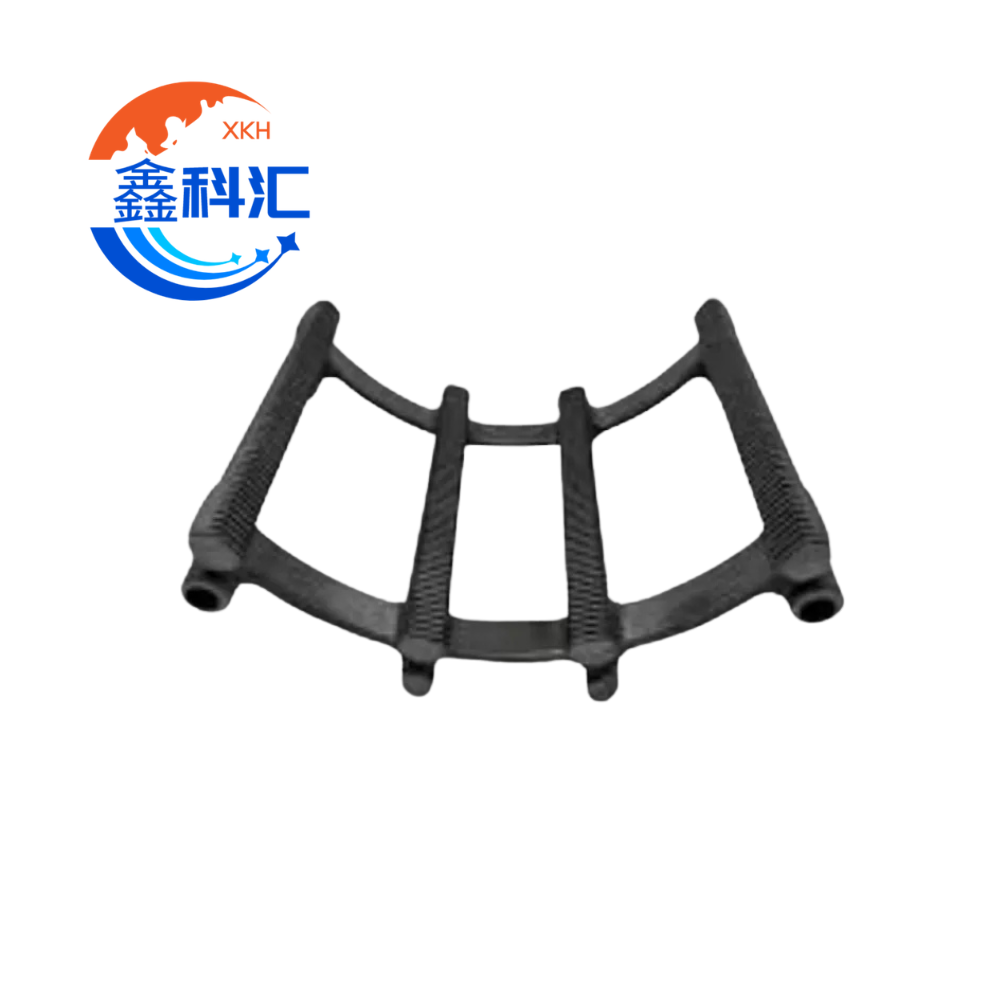
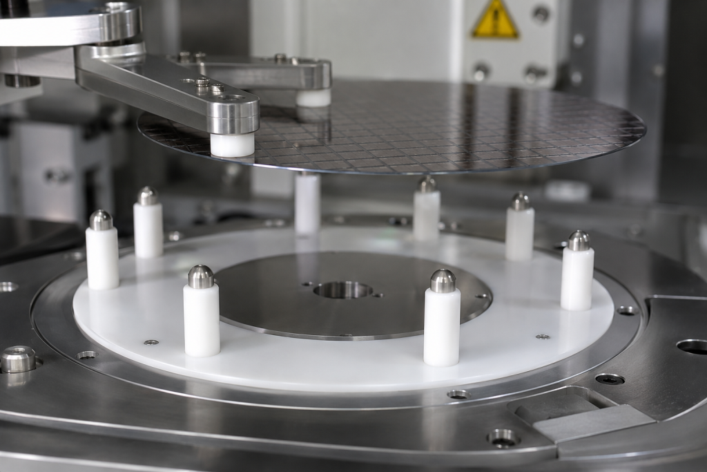
Ceramic Wafer Support Pins: Material Selection, Flatness and Particle Control

Ceramic wafer support pins are small but critical components in semiconductor processing equipment. They support, lift, position or temporarily separate wafers during transfer between a robot arm, process chamber, electrostatic chuck, vacuum chuck or wafer stage. Although their geometry is relatively simple, wafer support pins directly contact or approach sensitive wafer surfaces. Variations in pin […]

Ceramic Wafer Support Pins: Material Selection, Flatness and Particle Control Läs mer »
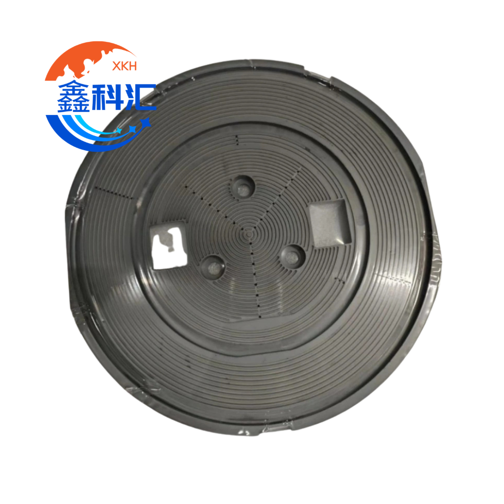
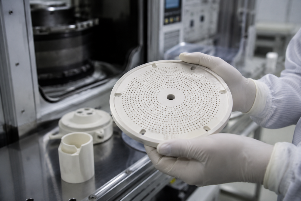
Ceramic Vacuum Chuck Design: Porosity, Flatness and Wafer Holding Performance

Vacuum chucks are essential components in modern semiconductor manufacturing. They securely hold silicon, silicon carbide (SiC), sapphire, glass, and compound semiconductor wafers during lithography, inspection, grinding, polishing, laser processing, metrology, and wafer bonding. Among various chuck technologies, porous ceramic vacuum chuck have become the preferred solution because they provide uniform vacuum distribution, excellent dimensional stability,

Ceramic Vacuum Chuck Design: Porosity, Flatness and Wafer Holding Performance Läs mer »

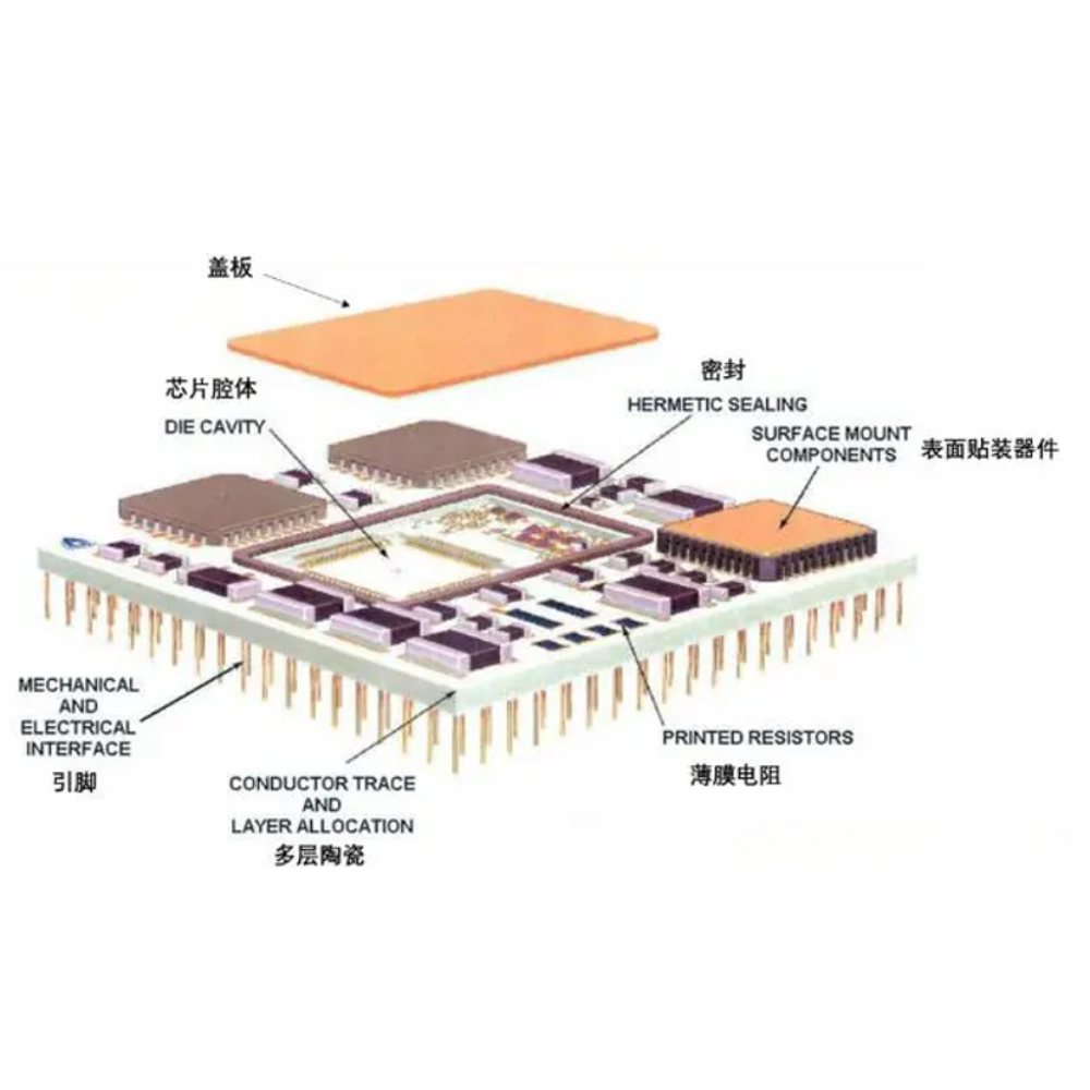
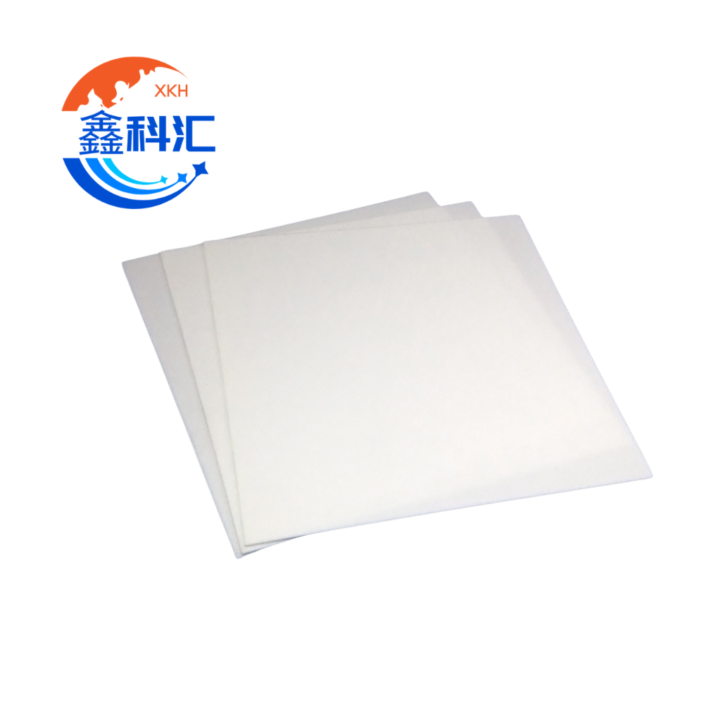
Ceramic Substrates: The Thermal Management Backbone of Advanced Electronic Devices

As emerging technologies such as electric vehicles (EVs), 5G communications, renewable energy systems, artificial intelligence (AI), aerospace electronics, and power semiconductors continue to evolve, electronic devices are becoming increasingly powerful, compact, and highly integrated. While these advancements improve performance, they also generate significantly higher heat densities, creating critical challenges for thermal management and device reliability.

Ceramic Substrates: The Thermal Management Backbone of Advanced Electronic Devices Läs mer »

6 viktiga keramiska substratmaterial förklarade: En omfattande guide

With the rapid development of electric vehicles, power electronics, aerospace systems, satellite communications, and high-frequency semiconductor devices, electronic components are increasingly required to operate under high power, high temperature, and high frequency conditions. In such demanding environments, traditional organic or metal-based substrates often fail to provide sufficient thermal and electrical stability. As a result, advanced

6 viktiga keramiska substratmaterial förklarade: En omfattande guide Läs mer »

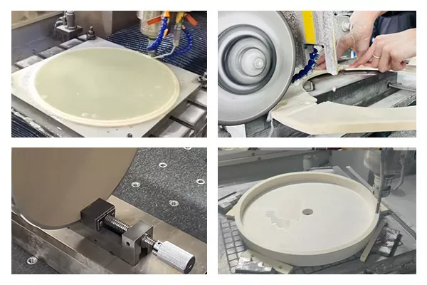
Tillverkningsprocess för keramiska komponenter för halvledare: Från råpulver till precisionsdelar

Modern semiconductor manufacturing relies heavily on advanced equipment such as etching systems, lithography machines, ion implantation tools, and deposition equipment. Inside these systems, numerous ceramic components play critical roles in ensuring process stability, precision, and reliability. Thanks to their exceptional high-temperature resistance, corrosion resistance, mechanical strength, dimensional stability, and electrical properties, advanced ceramic components are

Tillverkningsprocess för keramiska komponenter för halvledare: Från råpulver till precisionsdelar Läs mer »

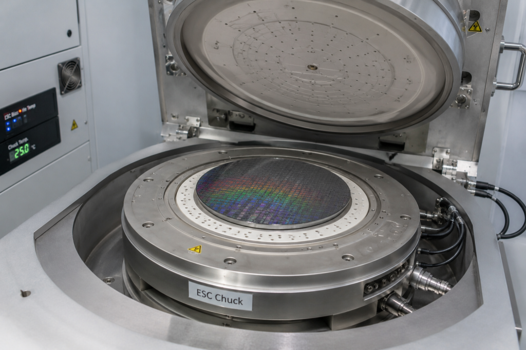
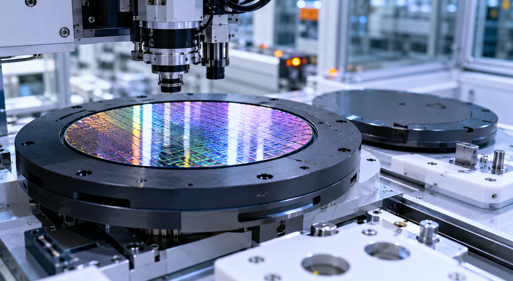
Elektrostatisk chuck vs vakuumchuck: Vilken teknik för att hålla wafers är bäst för halvledartillverkning?

In semiconductor manufacturing, wafer positioning and fixation are fundamental requirements for achieving process precision and yield stability. During etching, deposition, lithography, inspection, and plasma processing, silicon wafers must remain securely held while maintaining minimal contamination and excellent thermal uniformity. As device structures continue shrinking and wafer sizes continue increasing, traditional holding methods face growing challenges.

Elektrostatisk chuck vs vakuumchuck: Vilken teknik för att hålla wafers är bäst för halvledartillverkning? Läs mer »

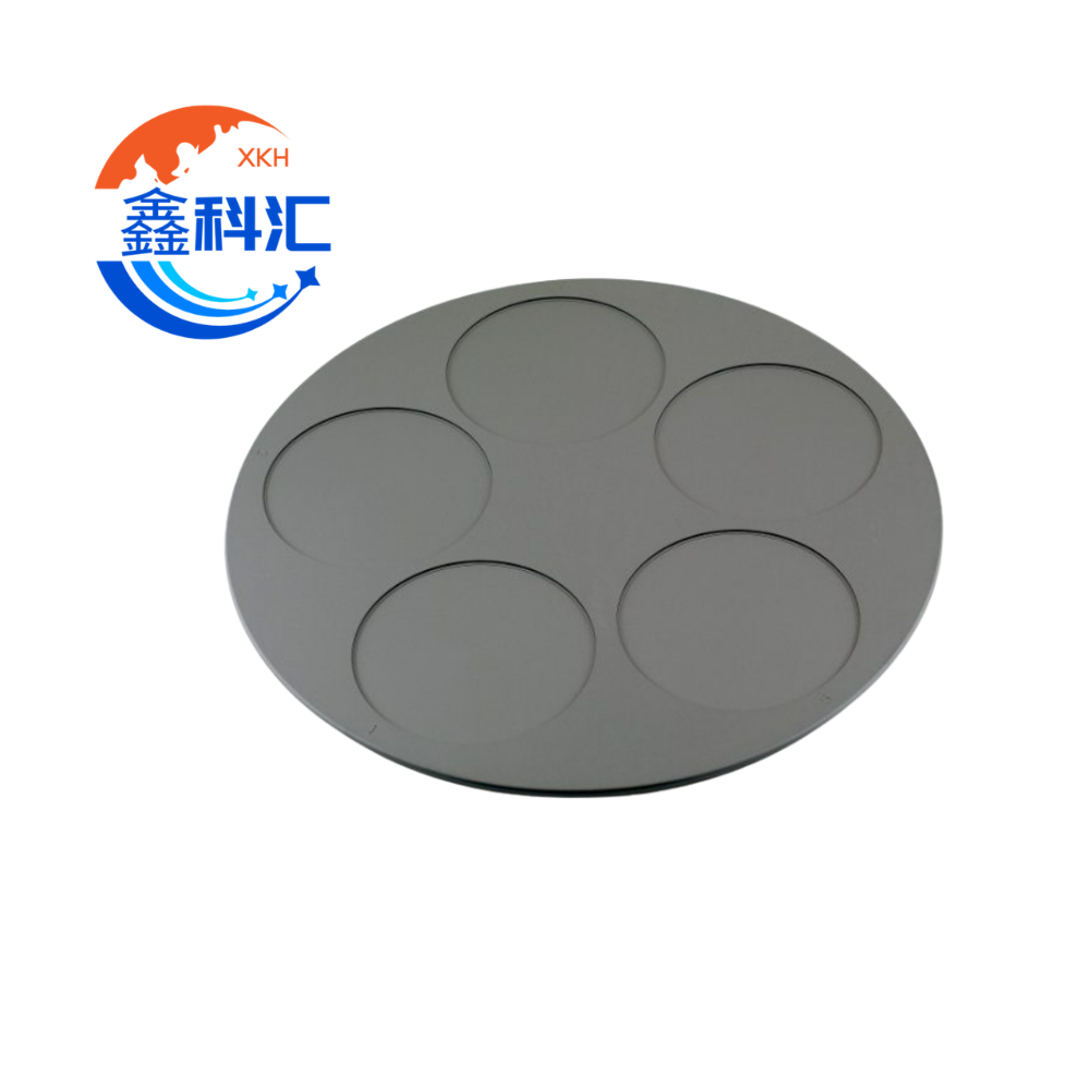
Varför kiselkarbidtråg ersätter traditionella waferbärare

As semiconductor manufacturing continues moving toward larger wafer sizes, higher process temperatures, and stricter contamination standards, conventional wafer carrier materials are increasingly reaching their performance limits. Components that once met process requirements are now facing challenges involving thermal deformation, particle generation, and shorter service life. Among advanced ceramic materials, silicon carbide (SiC) trays have emerged

Varför kiselkarbidtråg ersätter traditionella waferbärare Läs mer »

Keramisk kylfläns vs keramisk värmespridare: Viktiga skillnader och tekniska roller

In high-power electronics, semiconductor packaging, LED systems, and RF devices, thermal management is one of the most critical factors affecting performance and reliability. As power density continues to increase, two terms are frequently used: Ceramic Heatsink and Ceramic Heat Spreader. Although they sound similar, they serve very different roles in a thermal system. In simple

Keramisk kylfläns vs keramisk värmespridare: Viktiga skillnader och tekniska roller Läs mer »

Från litografi till tillverkning av wafers: Hur kiselkarbidkeramik driver en halvledarmarknad värd miljarder dollar

When people think about the semiconductor industry, they usually focus on chips, wafers, or advanced process nodes. However, behind every semiconductor breakthrough lies a less visible but equally critical foundation: advanced materials. As semiconductor manufacturing continues to pursue higher precision, smaller geometries, and faster production speeds, equipment performance requirements are becoming increasingly demanding. This shift

Från litografi till tillverkning av wafers: Hur kiselkarbidkeramik driver en halvledarmarknad värd miljarder dollar Läs mer »

Kiselkarbid Wafer Boat vs Quartz Wafer Boat: Vilket är bättre?

In semiconductor manufacturing, wafer handling components directly affect process stability, yield, and long-term operating cost. Among them, wafer boats play a critical role in transporting and supporting wafers during high-temperature diffusion, oxidation, epitaxy, and coating processes. Two of the most commonly used materials are Silicon Carbide (SiC) wafer boats and Quartz wafer boats. While both

Kiselkarbid Wafer Boat vs Quartz Wafer Boat: Vilket är bättre? Läs mer »

Tillverkningsutmaningar för keramiska komponenter med komplex struktur för halvledarutrustning

Vid avancerad halvledartillverkning arbetar viktiga processmoduler som plasmaetsning, kemisk förångningsdeposition (CVD) och jonimplantation i extrema miljöer med högenergiplasma, korrosiva gaser, högspänningsbias och snabba termiska cykler. Dessa förhållanden ställer höga krav på konstruktionsmaterialen när det gäller dielektrisk stabilitet, korrosionsbeständighet, termisk kompatibilitet och långsiktig dimensionell tillförlitlighet.

Tillverkningsutmaningar för keramiska komponenter med komplex struktur för halvledarutrustning Läs mer »

Funktionell keramik förklarad: En vetenskaplig översikt av avancerade tekniska material

1. Introduction Functional ceramics are a class of inorganic, non-metallic materials designed not only for structural integrity but also for specific physical, chemical, electrical, optical, or thermal functions. Unlike traditional ceramics used mainly for bricks, tiles, or sanitary ware, functional ceramics are engineered at the microstructural level to deliver targeted performance in advanced technologies. They

Funktionell keramik förklarad: En vetenskaplig översikt av avancerade tekniska material Läs mer »