업계 뉴스

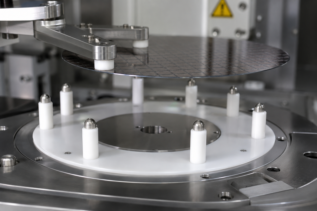
Ceramic Wafer Support Pins: Material Selection, Flatness and Particle Control

Ceramic wafer support pins are small but critical components in semiconductor processing equipment. They support, lift, position or temporarily separate wafers during transfer between a robot arm, process chamber, electrostatic chuck, vacuum chuck or wafer stage. Although their geometry is relatively simple, wafer support pins directly contact or approach sensitive wafer surfaces. Variations in pin […]

Ceramic Wafer Support Pins: Material Selection, Flatness and Particle Control 더 읽기"
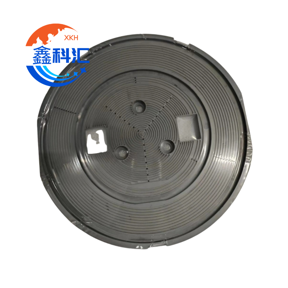
Ceramic Vacuum Chuck Design: Porosity, Flatness and Wafer Holding Performance

Vacuum chucks are essential components in modern semiconductor manufacturing. They securely hold silicon, silicon carbide (SiC), sapphire, glass, and compound semiconductor wafers during lithography, inspection, grinding, polishing, laser processing, metrology, and wafer bonding. Among various chuck technologies, porous ceramic vacuum chuck have become the preferred solution because they provide uniform vacuum distribution, excellent dimensional stability,

Ceramic Vacuum Chuck Design: Porosity, Flatness and Wafer Holding Performance 더 읽기"

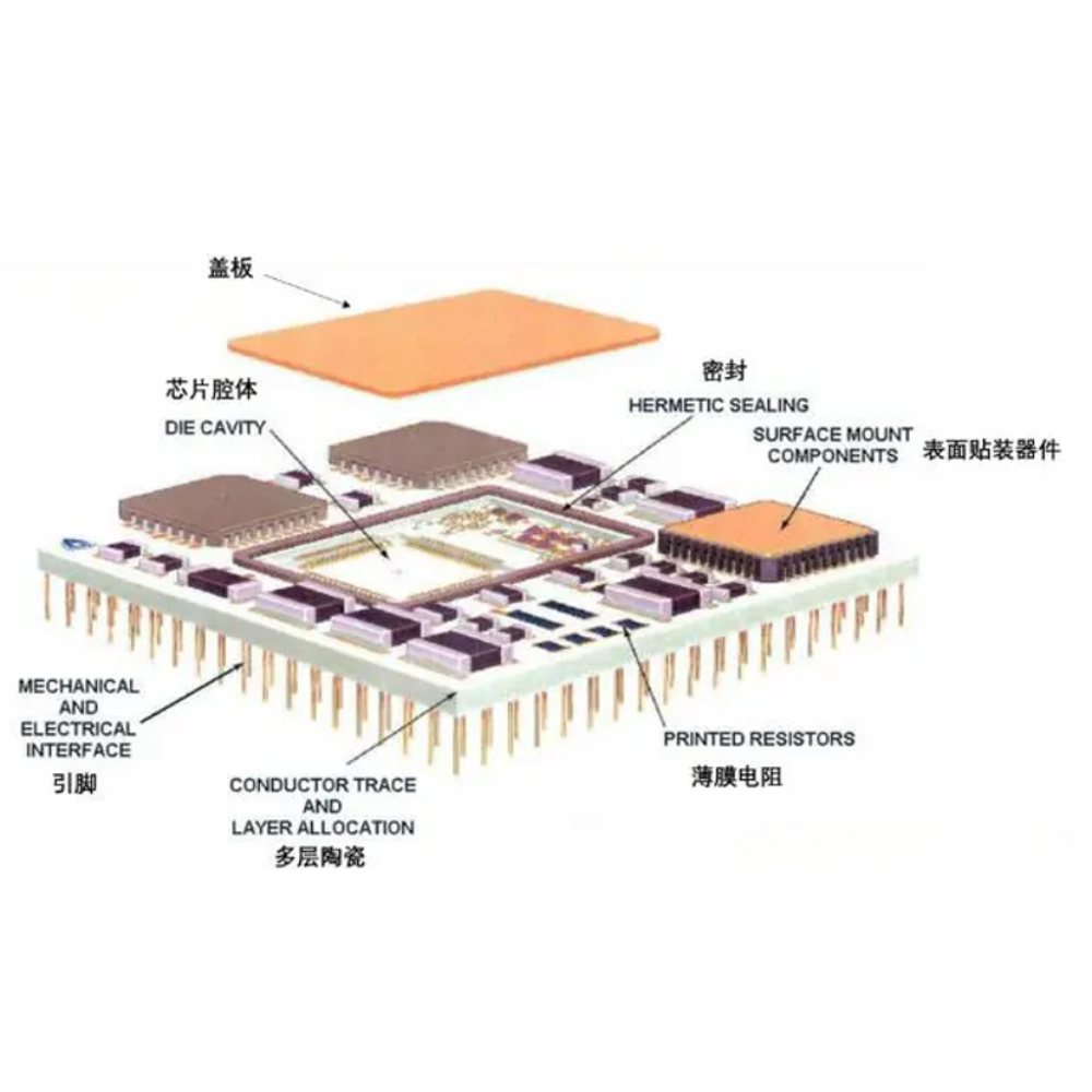
Ceramic Substrates: The Thermal Management Backbone of Advanced Electronic Devices

As emerging technologies such as electric vehicles (EVs), 5G communications, renewable energy systems, artificial intelligence (AI), aerospace electronics, and power semiconductors continue to evolve, electronic devices are becoming increasingly powerful, compact, and highly integrated. While these advancements improve performance, they also generate significantly higher heat densities, creating critical challenges for thermal management and device reliability.

Ceramic Substrates: The Thermal Management Backbone of Advanced Electronic Devices 더 읽기"

6가지 주요 세라믹 기판 소재 해설: 종합 가이드

With the rapid development of electric vehicles, power electronics, aerospace systems, satellite communications, and high-frequency semiconductor devices, electronic components are increasingly required to operate under high power, high temperature, and high frequency conditions. In such demanding environments, traditional organic or metal-based substrates often fail to provide sufficient thermal and electrical stability. As a result, advanced

6가지 주요 세라믹 기판 소재 해설: 종합 가이드 더 읽기"

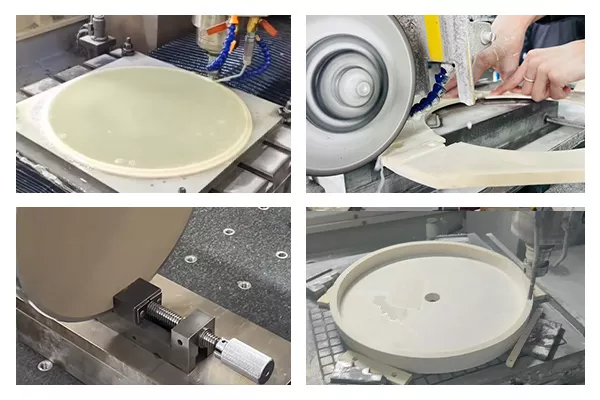
반도체 세라믹 부품 제조 공정: 원료 분말부터 정밀 부품까지

Modern semiconductor manufacturing relies heavily on advanced equipment such as etching systems, lithography machines, ion implantation tools, and deposition equipment. Inside these systems, numerous ceramic components play critical roles in ensuring process stability, precision, and reliability. Thanks to their exceptional high-temperature resistance, corrosion resistance, mechanical strength, dimensional stability, and electrical properties, advanced ceramic components are

반도체 세라믹 부품 제조 공정: 원료 분말부터 정밀 부품까지 더 읽기"

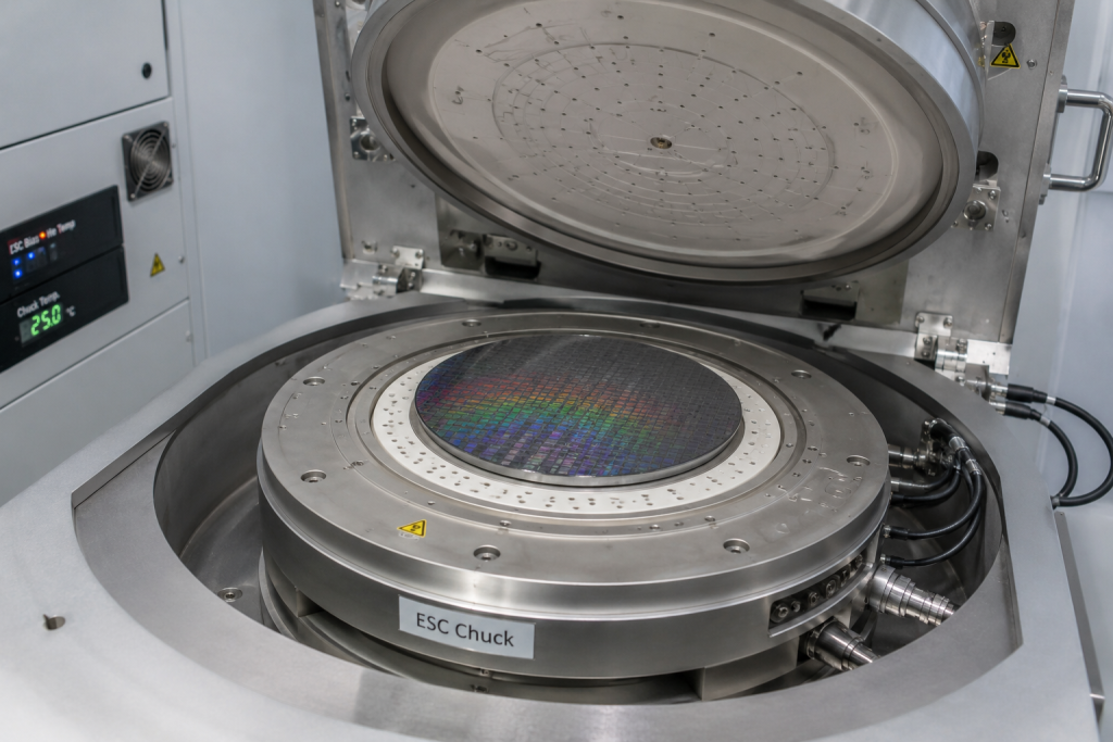
정전기 척과 진공 척: 반도체 제조에 더 적합한 웨이퍼 고정 기술은 무엇일까요?

In semiconductor manufacturing, wafer positioning and fixation are fundamental requirements for achieving process precision and yield stability. During etching, deposition, lithography, inspection, and plasma processing, silicon wafers must remain securely held while maintaining minimal contamination and excellent thermal uniformity. As device structures continue shrinking and wafer sizes continue increasing, traditional holding methods face growing challenges.

정전기 척과 진공 척: 반도체 제조에 더 적합한 웨이퍼 고정 기술은 무엇일까요? 더 읽기"

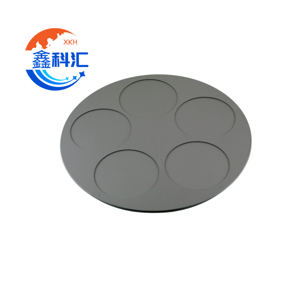
실리콘 카바이드 트레이가 기존 웨이퍼 캐리어를 대체하는 이유

As semiconductor manufacturing continues moving toward larger wafer sizes, higher process temperatures, and stricter contamination standards, conventional wafer carrier materials are increasingly reaching their performance limits. Components that once met process requirements are now facing challenges involving thermal deformation, particle generation, and shorter service life. Among advanced ceramic materials, silicon carbide (SiC) trays have emerged

실리콘 카바이드 트레이가 기존 웨이퍼 캐리어를 대체하는 이유 더 읽기"

세라믹 방열판과 세라믹 히트 스프레더: 주요 차이점 및 엔지니어링 역할

In high-power electronics, semiconductor packaging, LED systems, and RF devices, thermal management is one of the most critical factors affecting performance and reliability. As power density continues to increase, two terms are frequently used: Ceramic Heatsink and Ceramic Heat Spreader. Although they sound similar, they serve very different roles in a thermal system. In simple

세라믹 방열판과 세라믹 히트 스프레더: 주요 차이점 및 엔지니어링 역할 더 읽기"

리소그래피에서 웨이퍼 제조까지: 실리콘 카바이드 세라믹이 10억 달러 규모의 반도체 시장을 이끄는 방법

When people think about the semiconductor industry, they usually focus on chips, wafers, or advanced process nodes. However, behind every semiconductor breakthrough lies a less visible but equally critical foundation: advanced materials. As semiconductor manufacturing continues to pursue higher precision, smaller geometries, and faster production speeds, equipment performance requirements are becoming increasingly demanding. This shift

리소그래피에서 웨이퍼 제조까지: 실리콘 카바이드 세라믹이 10억 달러 규모의 반도체 시장을 이끄는 방법 더 읽기"

실리콘 카바이드 웨이퍼 보트 대 석영 웨이퍼 보트: 어느 것이 더 낫습니까?

In semiconductor manufacturing, wafer handling components directly affect process stability, yield, and long-term operating cost. Among them, wafer boats play a critical role in transporting and supporting wafers during high-temperature diffusion, oxidation, epitaxy, and coating processes. Two of the most commonly used materials are Silicon Carbide (SiC) wafer boats and Quartz wafer boats. While both

실리콘 카바이드 웨이퍼 보트 대 석영 웨이퍼 보트: 어느 것이 더 낫습니까? 더 읽기"

반도체 장비를 위한 복잡한 구조의 세라믹 부품 제조 과제

첨단 반도체 제조에서 플라즈마 식각, 화학 기상 증착(CVD), 이온 주입과 같은 주요 공정 모듈은 고에너지 플라즈마, 부식성 가스, 고전압 바이어스, 빠른 열 순환과 같은 극한의 환경에서 작동합니다. 이러한 조건은 유전체 안정성, 내식성, 열 호환성 및 장기 치수 신뢰성 측면에서 구조 재료에 엄격한 요구 사항을 부과합니다.

반도체 장비를 위한 복잡한 구조의 세라믹 부품 제조 과제 더 읽기"

기능성 세라믹 설명: 첨단 엔지니어링 소재에 대한 과학적 개요

1. Introduction Functional ceramics are a class of inorganic, non-metallic materials designed not only for structural integrity but also for specific physical, chemical, electrical, optical, or thermal functions. Unlike traditional ceramics used mainly for bricks, tiles, or sanitary ware, functional ceramics are engineered at the microstructural level to deliver targeted performance in advanced technologies. They

기능성 세라믹 설명: 첨단 엔지니어링 소재에 대한 과학적 개요 더 읽기"