
Semiconductor manufacturing equipment operates under some of the most demanding conditions found in modern industrial production. Components may be exposed to high temperatures, plasma, corrosive gases, vacuum environments, rapid thermal cycling, aggressive cleaning processes and extremely strict contamination requirements.
Under these conditions, conventional metals and polymers are not always suitable. This is why structural ceramics are widely used in semiconductor manufacturing equipment, particularly for wafer handling, plasma processing, thermal processing, precision positioning and electrical insulation.
Materials such as alumina, aluminum nitride, silicon carbide and zirconia provide a combination of mechanical strength, thermal stability, electrical properties and chemical resistance that can help improve equipment reliability and reduce particle contamination.
This guide explains the main structural ceramic materials used in semiconductor manufacturing, their key properties and typical applications.
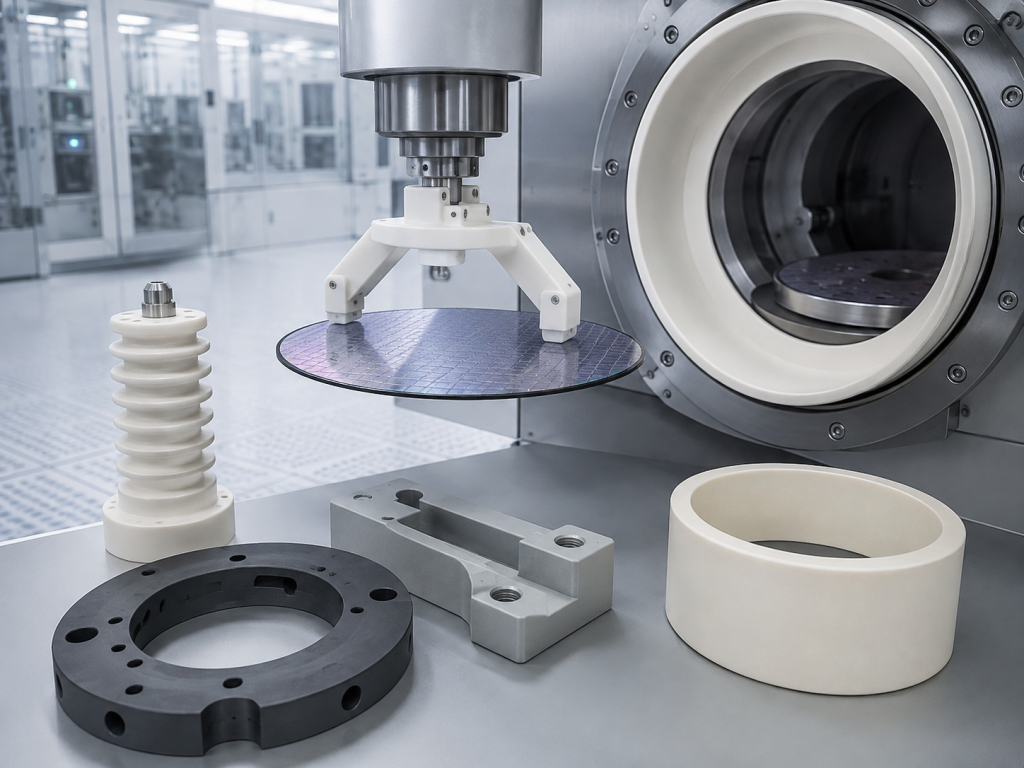
What Are Structural Ceramics?
Structural ceramics are advanced ceramic materials engineered primarily for mechanical, thermal and functional performance rather than decorative applications.
Unlike conventional pottery or building ceramics, semiconductor-grade structural ceramics are manufactured using carefully controlled powders, forming processes, sintering conditions and precision machining.
Common structural ceramic materials include:
- Alumina ceramic
- Aluminum nitride ceramic
- Silicon carbide ceramic
- Zirconia ceramic
- Silicon nitride ceramic
Depending on the process environment, ceramic components can be manufactured as:
- Wafer handling parts
- Ceramic arms and end effectors
- Vacuum components
- Insulating components
- Plasma chamber parts
- Ceramic rings
- Precision positioning components
- Heating and thermal management parts
- Structural supports
- Customized equipment components
Material selection depends heavily on the operating environment.
Why Are Structural Ceramics Used in Semiconductor Equipment?
Semiconductor manufacturing requires extremely stable components because even small dimensional changes, particles or contamination can influence wafer yield.
Structural ceramics offer several important advantages.
High Mechanical Stability
Many advanced ceramics maintain excellent rigidity under mechanical loads.
Low deformation is particularly important for components involved in:
- Wafer positioning
- Robotic wafer transfer
- Precision alignment
- Vacuum handling
- Inspection equipment
Ceramic materials can maintain dimensional stability even when components are thin or exposed to repeated operating cycles.
High Temperature Resistance
Certain semiconductor processes operate at temperatures far beyond the practical operating range of many polymers and metals.
Ceramics can maintain structural stability under elevated temperatures, making them suitable for applications such as:
- Diffusion furnaces
- Annealing systems
- Deposition equipment
- High-temperature wafer processing
- Thermal treatment systems
The exact temperature capability depends on the ceramic material and manufacturing process.
Excellent Electrical Insulation
Alumina and aluminum nitride provide excellent electrical insulation.
They are therefore commonly used for:
- Electrical isolation
- Sensor substrates
- Heater components
- High-voltage insulation
- Semiconductor processing equipment
Electrical resistivity, dielectric strength and dielectric constant should be considered when selecting a ceramic for electrical applications.
Plasma and Chemical Resistance
Plasma processing is widely used during semiconductor etching, deposition and chamber cleaning.
Components located near the plasma environment may experience:
- Ion bombardment
- Chemical corrosion
- Surface erosion
- Particle generation
Materials such as alumina, silicon carbide and other engineered ceramics can provide improved durability compared with conventional materials in certain plasma environments.
Low Contamination Potential
Contamination control is one of the most important considerations in semiconductor manufacturing.
Ceramic purity, secondary phases, grain structure and surface condition can all influence contamination performance.
For critical semiconductor applications, buyers often specify:
- High material purity
- Controlled trace metal content
- Tight dimensional tolerance
- Low surface roughness
- Clean packaging
- Controlled cleaning procedures
Alumina Ceramic
Alumina (Al₂O₃) is one of the most widely used structural ceramic materials in semiconductor equipment.
Typical grades include:
- 95% alumina
- 96% alumina
- 99% alumina
- 99.5% alumina
- 99.7% or higher-purity alumina
Higher-purity grades are generally preferred for applications where contamination control is critical.
Key Properties
Alumina provides:
- High hardness
- Excellent electrical insulation
- Good mechanical strength
- Good chemical resistance
- High temperature capability
- Good wear resistance
- Relatively mature manufacturing technology
Semiconductor Applications
Common applications include:
- Ceramic insulators
- Wafer handling components
- Ceramic rings
- Vacuum components
- Positioning parts
- Chamber components
- Electrical feedthrough components
- Precision structural components
Alumina is often selected when a balance between performance, machinability and cost is required.
Aluminum Nitride Ceramic
Aluminum nitride (AlN) is particularly valuable when both electrical insulation and thermal conductivity are required.
Compared with conventional alumina, AlN can provide significantly higher thermal conductivity while maintaining good electrical insulation.
Key Properties
AlN typically offers:
- High thermal conductivity
- Electrical insulation
- Relatively low thermal expansion
- Good thermal shock behavior
- Good dimensional stability
Semiconductor Applications
Typical uses include:
- Semiconductor heater components
- Electrostatic chuck-related components
- Thermal management components
- Power semiconductor substrates
- Equipment components requiring heat dissipation
- High-performance electronic packaging
One important consideration is moisture sensitivity during storage and processing. Proper surface treatment, cleaning and packaging are therefore important.
Silicon Carbide Ceramic
Silicon carbide (SiC) combines excellent mechanical strength with outstanding thermal and chemical properties.
Different manufacturing technologies produce SiC materials with different densities, purities and microstructures.
Examples include:
- Sintered silicon carbide
- Reaction-bonded silicon carbide
- CVD silicon carbide
- Recrystallized silicon carbide
Key Properties
SiC offers:
- High hardness
- Excellent wear resistance
- High thermal conductivity
- Low thermal expansion
- Excellent thermal shock resistance
- High temperature stability
- Good resistance to many corrosive environments
Semiconductor Applications
SiC ceramic components can be used for:
- Wafer carriers
- Wafer boats
- Process chamber components
- Etching equipment parts
- High-temperature fixtures
- Precision stages
- Structural supports
For extremely high-purity environments, the specific SiC manufacturing method becomes particularly important.
Zirconia Ceramic
Zirconia (ZrO₂) differs from many other technical ceramics because of its relatively high fracture toughness.
It can tolerate mechanical impact and localized stress better than many brittle ceramic materials.
Key Properties
Zirconia provides:
- High fracture toughness
- Excellent wear resistance
- High mechanical strength
- Good surface finishing capability
- Low thermal conductivity
- Excellent dimensional precision after machining
Semiconductor Applications
Zirconia can be used for:
- Precision positioning components
- Wear-resistant parts
- Ceramic pins
- Alignment components
- Small mechanical components
- Precision fixtures
- Moving equipment components
It is particularly useful where both wear resistance and mechanical toughness are required.
Silicon Nitride Ceramic
Silicon nitride is another high-performance structural ceramic used in demanding mechanical environments.
Key Properties
Silicon nitride provides:
- High fracture toughness
- High strength
- Excellent thermal shock resistance
- Good wear resistance
- Low density
- High temperature stability
Because of these characteristics, it may be used for precision mechanical components that experience repeated mechanical or thermal loading.
Structural Ceramic Material Comparison
| Material | Main Advantage | Typical Semiconductor Application |
|---|---|---|
| Alumina | Electrical insulation and cost-performance balance | Insulators, structural parts, chamber components |
| Aluminum Nitride | High thermal conductivity with electrical insulation | Heaters, thermal management components |
| Silicon Carbide | Thermal stability and plasma/chemical resistance | Wafer carriers, chamber and process parts |
| Zirconia | High toughness and wear resistance | Precision mechanical and positioning parts |
| Silicon Nitride | Strength and thermal shock resistance | High-load precision structural components |
No single ceramic material is ideal for every semiconductor process.
The correct choice depends on the operating conditions of the equipment.
Important Specifications When Ordering Semiconductor Ceramic Parts
For custom ceramic components, simply specifying the ceramic material is usually not sufficient.
A complete RFQ should ideally include the following information.
Material and Purity
Specify the exact ceramic type and required purity whenever possible.
For example:
Al₂O₃ ≥99.5%
rather than simply stating:
Alumina ceramic
This is especially important for semiconductor applications where trace contamination must be controlled.
Dimensions and Tolerances
Provide complete engineering drawings showing:
- Diameter
- Length
- Width
- Thickness
- Hole dimensions
- Groove dimensions
- Flatness
- Parallelism
- Perpendicularity
- Position tolerance
Ceramics behave differently from metals during machining, so tolerance requirements can significantly affect manufacturing difficulty and cost.
Surface Roughness
Surface roughness may influence:
- Particle generation
- Vacuum sealing
- Wafer contact
- Friction
- Cleaning performance
- Plasma interaction
Typical drawings may specify requirements such as:
Ra ≤0.8 μm
or significantly lower values for precision polished surfaces.
Surface Finish
Different areas of the same component may require different surface treatments.
These can include:
- As-fired
- Ground
- Lapped
- Polished
- Mirror polished
Only critical areas should normally receive extremely tight surface specifications because unnecessary polishing can increase manufacturing cost.
Operating Environment
The supplier should understand whether the component will operate in:
- Vacuum
- Plasma
- High temperature
- Corrosive gas
- Chemical cleaning
- Repeated thermal cycling
- High-voltage environments
This information helps determine the most suitable material and manufacturing process.
Ceramic Machining for Semiconductor Components
Advanced ceramic components are typically produced through several manufacturing stages.
A typical process may include:
Powder preparation → forming → sintering → grinding → precision machining → polishing → cleaning → inspection
Because fully sintered ceramics are extremely hard, precision machining commonly requires diamond tooling.
Possible machining capabilities include:
- CNC grinding
- Surface grinding
- Cylindrical grinding
- Drilling
- Slot machining
- Precision lapping
- Polishing
- Complex geometry machining
For semiconductor applications, machining quality must be controlled carefully because microcracks, edge defects and surface damage may shorten component lifetime.
Particle Control and Surface Quality
A ceramic part may meet dimensional specifications but still perform poorly if its surface produces particles during use.
Potential particle sources include:
- Rough machined surfaces
- Microcracks
- Edge chipping
- Weak grain boundaries
- Residual machining contamination
- Improper cleaning
For critical wafer-handling and chamber components, edge finishing and surface inspection should therefore be included in the quality control process.
Inspection Requirements
Depending on the application, semiconductor ceramic components may require inspection for:
- Dimensional accuracy
- Flatness
- Parallelism
- Surface roughness
- Visual defects
- Edge chipping
- Material density
- Material purity
- Mechanical properties
- Electrical properties
Coordinate measuring machines, optical inspection systems and surface profilometers may be used for precision components.
How to Choose the Right Structural Ceramic
The most effective approach is to select the material based on the operating environment rather than selecting ceramics based only on price.
For example:
If electrical insulation is the primary requirement, alumina may be appropriate.
If both electrical insulation and high thermal conductivity are required, aluminum nitride should be considered.
If the component operates in a high-temperature or aggressive process environment, silicon carbide may offer better performance.
If the component requires high toughness and wear resistance, zirconia may be more suitable.
Engineering drawings, operating temperature, chemical environment, dimensional tolerances and contamination requirements should therefore be evaluated together before selecting the material.
Custom Structural Ceramic Components for Semiconductor Equipment
Semiconductor equipment manufacturers increasingly require customized ceramic components rather than standard ceramic shapes.
Typical custom requirements include:
- Complex geometries
- Thin-wall structures
- Precision holes and slots
- Tight flatness requirements
- High-purity materials
- Low surface roughness
- Customized cleaning and packaging
- Prototype and small-batch manufacturing
Early communication between equipment designers and ceramic manufacturers can help optimize the component for both performance and manufacturability.
Conclusion
Structural ceramics play an increasingly important role in semiconductor manufacturing because they can operate reliably in environments involving high temperature, plasma, vacuum, electrical insulation requirements and strict contamination control.
Alumina, aluminum nitride, silicon carbide, zirconia and silicon nitride each provide different advantages.
The most suitable material should be selected according to:
- Operating temperature
- Thermal conductivity
- Electrical properties
- Mechanical load
- Plasma exposure
- Chemical environment
- Surface requirements
- Purity requirements
- Dimensional tolerances
For custom semiconductor ceramic components, providing complete engineering drawings and process conditions allows manufacturers to recommend the appropriate material, machining method and inspection requirements.
XKH Ceramics provides precision ceramic machining and customized technical ceramic components for semiconductor equipment and other high-performance industrial applications. Customers can submit drawings, material requirements, tolerances, quantities and operating conditions for technical evaluation and quotation.

