
1. Introduction: Role of Advanced Ceramics in Semiconductor Equipment
In modern semiconductor manufacturing, equipment operates under extreme conditions such as vacuum environments, high temperatures, plasma exposure, and ultra-precision motion control. Traditional metallic materials often fail to meet the combined requirements of stability, cleanliness, electrical insulation, and thermal management.
Advanced engineering ceramics—such as alumina (Al₂O₃), aluminum nitride (AlN), and silicon carbide (SiC)—have therefore become essential materials for critical semiconductor components. After precision forming and ultra-precision machining, these ceramics are widely used in key process equipment including lithography, etching, thin-film deposition, ion implantation, and chemical mechanical planarization (CMP).
Among these components, the electrostatic chuck (ESC) represents one of the most important functional ceramic-based devices.
2. Function and Application of Electrostatic Chucks
An electrostatic chuck is a wafer handling and holding device designed for vacuum or plasma environments. It enables stable and uniform clamping of ultra-thin semiconductor wafers without mechanical contact.
It is widely used in advanced semiconductor processes such as:
- Plasma etching (ETCH)
- Physical vapor deposition (PVD)
- Plasma-enhanced chemical vapor deposition (PECVD)
- Extreme ultraviolet lithography (EUVL)
- Ion implantation
In these processes, wafers are exposed to energetic particles and thermal loads. Therefore, the electrostatic chuck must ensure both mechanical stability and precise thermal control.
3. Working Principle: Electrostatic Force and Thermal Management
The electrostatic chuck operates based on electrostatic attraction generated by an electric field. Oppositely charged surfaces create an attractive force that securely holds the wafer in place.
The fundamental electrostatic interaction can be described as:
F=kr2q1q2
q1
q2
r
F=kr2q1q2≈−5.06+-
Where:
- F: electrostatic force
- q1,q2: electric charges
- r: distance between charges
- k: Coulomb constant
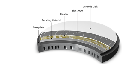
Structurally, an electrostatic chuck typically consists of three layers:
- Dielectric layer: defines insulation and electric field distribution
- Electrode layer: generates the electrostatic field
- Base layer: provides mechanical support and heat conduction
To manage thermal loads during processing, helium back-side cooling is commonly introduced, improving heat transfer between the wafer and the chuck surface.
4. Classification: Coulomb-Type and Johnsen–Rahbek-Type ESC
Electrostatic chucks are generally classified into two types based on their dielectric behavior:
(1) Coulomb-Type ESC
This type relies purely on electrostatic force for wafer clamping. It features a simpler structure but provides relatively lower clamping force.
(2) Johnsen–Rahbek (J-R) Type ESC
This type introduces slight electrical conductivity within the dielectric layer, enhancing polarization effects and increasing clamping force.
Key advantages include:
- Higher clamping force at lower voltage
- Improved wafer contact stability
- Better performance in advanced semiconductor nodes
However, it requires higher material uniformity and more complex manufacturing processes.
5. Industry Development and Market Characteristics
Driven by the rapid expansion of semiconductor manufacturing capacity and the increasing demand for advanced nodes, the electrostatic chuck market continues to grow steadily.
Key industry characteristics include:
(1) High technological barriers
The technology integrates materials science, electrical engineering, thermal management, and ultra-precision machining.
(2) High market concentration
The global market is dominated by a limited number of advanced manufacturers with strong integration capabilities.
(3) Regional specialization
High-end design and system integration are concentrated in technologically advanced regions, while precision ceramic manufacturing is increasingly shifting toward Asia.
(4) Growing localization trend
With the expansion of domestic semiconductor ecosystems, localized production of electrostatic chucks has begun to emerge, although challenges remain in long-term reliability and high-end process compatibility.
6. Key Materials and Future Development Trends
Future development of electrostatic chucks and ceramic components will focus on:
(1) High thermal conductivity ceramics
Improving temperature uniformity through optimized AlN and SiC materials.
(2) Ultra-high purity and low defect density
Reducing impurities and micro-defects to improve plasma resistance and stability.
(3) Multilayer composite structures
Balancing electrical insulation, mechanical strength, and thermal performance.
(4) Extended service life
Enhancing resistance to thermal cycling and plasma corrosion to reduce replacement frequency.
7. Conclusion
Electrostatic chucks, as core ceramic functional components in semiconductor equipment, integrate advanced materials science, electrostatics, and thermal engineering. Their performance directly influences wafer processing precision and manufacturing yield.
As semiconductor processes continue to evolve toward higher precision and smaller nodes, demand for high-performance ceramic components will continue to grow, driving ongoing innovation in materials and manufacturing technologies.