
Ceramic substrates are widely used in power electronics, semiconductor equipment, automotive electronics, LED modules, industrial lasers and other applications that require electrical insulation together with effective heat dissipation.
However, selecting the ceramic material is only part of the design process.
The method used to create the metal circuit on the ceramic surface can have an equally important effect on:
- Current-carrying capability
- Heat dissipation
- Circuit resolution
- Copper thickness
- Thermal cycling reliability
- Bond strength
- Component size
- Manufacturing cost
Among the most common ceramic metallization technologies are DBC, AMB, DPC and thick-film metallization.
Although these processes can all create conductive circuits on ceramic substrates, they are designed for very different performance requirements.
This guide explains the differences and provides a practical framework for selecting the appropriate metallization process.
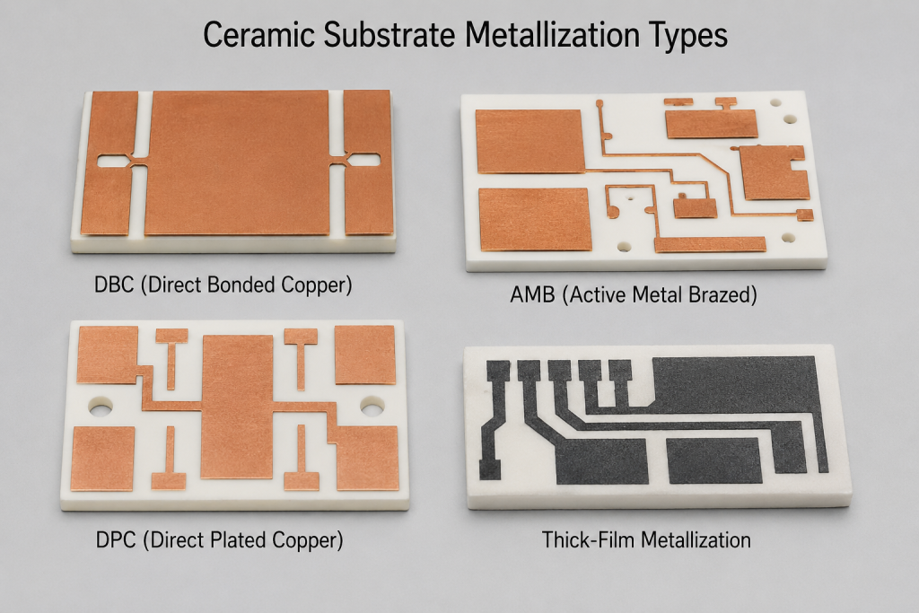
What Is Ceramic Substrate Metallization?
Technical ceramics such as alumina, aluminum nitride and silicon nitride provide excellent electrical insulation, but an untreated ceramic surface cannot function as an electrical circuit.
Metallization adds conductive areas such as:
- Circuit traces
- Bonding pads
- Power terminals
- Ground areas
- Soldering surfaces
- Resistor patterns
- Thermal spreading areas
to the ceramic substrate.
The challenge is that ceramics and metals have very different physical properties.
A successful metallization system must therefore maintain reliable adhesion while the component experiences temperature changes, mechanical stress and repeated operating cycles.
The most suitable process depends on the ceramic material, required metal thickness, circuit dimensions and final operating environment.
1. DBC — Direct Bonded Copper
DBC, also called Direct Bond Copper, is one of the most established metallization technologies for power electronic ceramic substrates.
In a DBC structure, copper foil is bonded directly to an electrically insulating ceramic substrate using a high-temperature bonding process. Rogers describes its DBC process as a high-temperature melting and diffusion process that bonds pure copper directly to ceramic.
Typical ceramic materials include:
- Al2O3 alumina
- AlN aluminum nitride
Commercial DBC products are widely used in power modules where thick copper conductors, electrical insulation and heat spreading are required.
Why DBC Is Popular
The major advantage of DBC is its ability to combine a relatively thick copper layer with an electrically insulating ceramic.
The copper can carry substantial current and spread heat laterally, while the ceramic provides electrical isolation between the electronic circuit and the baseplate or cooling system.
This combination makes DBC particularly suitable for:
- IGBT modules
- MOSFET power modules
- Power converters
- Motor drives
- Industrial power electronics
- Renewable-energy inverters
- Railway electronics
- Automotive power systems
Rogers specifically markets Al2O3 DBC for power applications and AlN DBC for applications with higher power density and more demanding thermal requirements.
DBC with Alumina vs AlN
The ceramic underneath the copper strongly affects thermal performance.
Al2O3 DBC
Alumina provides:
- Good electrical insulation
- Established manufacturing technology
- Good mechanical performance
- Relatively attractive cost
It is often selected when power density is moderate and cost is an important consideration.
CeramTec lists approximately 24 W/m·K thermal conductivity for representative alumina substrate material, although exact performance varies with grade.
AlN DBC
Aluminum nitride offers substantially higher thermal conductivity.
Commercial AlN substrates may provide thermal conductivity around 170 W/m·K or higher depending on the grade; MARUWA lists AlN grades in approximately the 170–230 W/m·K range.
AlN DBC is therefore attractive for:
- High-power-density modules
- SiC power devices
- GaN power devices
- High-power LEDs
- Laser modules
- Applications where junction temperature must be minimized
The tradeoff is generally higher material and processing cost.
2. AMB — Active Metal Brazed Ceramic Substrates
AMB stands for Active Metal Brazing.
Instead of using the same bonding mechanism as conventional DBC, AMB uses an active brazing system to join the metal layer to the ceramic.
This technique is especially important for ceramic materials such as silicon nitride (Si3N4).
Ferrotec, for example, offers AMB substrates based on AlN and Si3N4, while DBC products are commonly offered on alumina and AlN.
Why Si3N4 + AMB Is Important
Silicon nitride has become particularly attractive for high-reliability power modules because of its combination of:
- High flexural strength
- High fracture toughness
- Electrical insulation
- Useful thermal conductivity
- Strong resistance to mechanical and thermal stress
CeramTec reports representative Si3N4 substrate values of at least 700 MPa bending strength, fracture toughness of at least 6.5 MPa√m and thermal conductivity around 90 W/m·K.
This combination can be valuable in demanding applications such as:
- Electric vehicle traction inverters
- SiC power modules
- GaN power modules
- Railway converters
- Renewable-energy power modules
- High-reliability industrial drives
CeramTec specifically positions thin Si3N4 substrates combined with AMB metallization for wide-bandgap devices such as SiC and GaN.
3. DBC vs AMB
DBC and AMB are frequently compared because both can create thick-metal ceramic substrates for power electronics.
However, the correct choice depends heavily on the substrate material and reliability requirements.
| Parameter | DBC | AMB |
|---|---|---|
| Typical ceramic | Al2O3, AlN | Si3N4, AlN |
| Metal | Usually copper | Usually copper |
| Main strength | Mature, cost-effective thick copper system | High-reliability bonding for demanding ceramic systems |
| Thermal performance | Depends strongly on ceramic | Depends strongly on ceramic |
| Mechanical reliability | Good | Particularly attractive with high-toughness Si3N4 |
| Common application | General power electronics | Automotive and high-reliability power modules |
For applications where cost and established production are important, alumina DBC may be sufficient.
When very high power density, severe thermal cycling or mechanical reliability becomes critical, designers increasingly evaluate combinations such as:
Si3N4 + AMB.
The substrate should therefore be selected as a complete ceramic + metallization system, rather than selecting the ceramic and copper process separately.
4. DPC — Direct Plated Copper
DPC generally refers to Direct Plated Copper, where copper is built onto a metallized ceramic surface through deposition and plating processes rather than bonding a thick copper foil to the ceramic in the same way as DBC.
The exact process sequence can vary between manufacturers.
A typical concept may involve:
- Ceramic surface preparation
- Formation of an adhesion or seed layer
- Photolithographic circuit definition
- Copper plating
- Pattern formation
- Surface finishing
The primary advantage of this approach is greater flexibility for creating relatively precise circuit patterns.
MARUWA identifies DPC alongside DBC, AMB, thick-film and thin-film technologies as circuit options for ceramic substrates, including silicon nitride.
5. Where DPC Has an Advantage
DBC is highly effective when thick copper and high current are the main requirements.
DPC becomes more attractive when designers need:
- Finer conductor patterns
- Smaller pads
- Higher routing density
- More precise copper geometry
- Custom circuit layouts
- Plated vias
- Smaller electronic packages
Because its metallization is formed by patterning and plating processes, DPC can generally support more detailed circuit structures than traditional thick-copper DBC designs.
This makes it useful for applications such as:
- LED packages
- Laser diode substrates
- Power device submounts
- Sensors
- Precision electronic modules
- High-density ceramic circuits
However, achievable line width, spacing, copper thickness and via geometry are supplier- and process-dependent and should always be confirmed during design review.
6. Thick-Film Metallization
Thick-film metallization is a very different approach.
Instead of bonding or plating a large copper foil, a conductive paste is typically patterned onto the ceramic substrate, commonly using screen-printing methods, and subsequently fired at elevated temperature.
MARUWA describes its thick-film substrates as screen-printed and high-temperature-sintered structures using materials including alumina and AlN.
Thick-film technology can create:
- Conductive traces
- Bonding pads
- Resistors
- Electrodes
- Via connections
- Multilayer circuit structures
It remains widely useful where moderate conductor thickness and flexible circuit design are more important than the very high current capacity of thick copper DBC or AMB.
7. Advantages of Thick-Film Metallization
One major advantage is manufacturing flexibility.
Conductive and resistive functions can potentially be integrated into the same ceramic substrate.
Printed resistors can also be adjusted after firing using laser trimming. Kyocera describes ceramic substrates using printed resistors with laser trimming for accurate resistance adjustment.
Other advantages can include:
- Relatively economical manufacturing
- Flexible pattern design
- Integrated resistors
- Multilayer structures
- Via connections
- Compatibility with alumina and AlN
- Suitability for medium-volume customized circuits
MARUWA also notes that via structures can connect the top and bottom surfaces of thick-film ceramic substrates.
8. Thick Film vs DPC
Both technologies can be used for patterned ceramic circuits, but they target somewhat different requirements.
Thick Film
Best suited when:
- Circuit resolution is moderate
- Integrated resistors are useful
- Cost efficiency matters
- Screen-printable designs are acceptable
- High-current thick copper is unnecessary
DPC
More attractive when:
- Finer circuit geometry is needed
- Copper thickness must be controlled by plating
- Smaller bonding pads are required
- Precision circuit structures are important
- Higher packaging density is required
Therefore, the choice should not be based only on price.
The minimum required conductor width and spacing are often among the first parameters that determine whether thick film or a plated process is more appropriate.
9. DBC vs DPC
This is another common engineering comparison.
Choose DBC when the priority is:
- Thick copper
- High current
- Power electronics
- Efficient heat spreading
- High-voltage isolation
- Large power semiconductor dies
Consider DPC when the priority is:
- Finer patterns
- More compact circuits
- More flexible copper thickness
- Precise pad geometry
- High-density routing
A useful simplification is:
DBC = power first
DPC = pattern precision first
although real designs may involve additional tradeoffs.
10. AMB vs DPC
AMB is normally associated with thick-metal power substrates where mechanical and thermal cycling reliability are critical.
DPC generally targets more precise circuit structures.
Therefore:
AMB
is often evaluated for:
- EV traction inverters
- High-current SiC modules
- High-reliability power modules
- Severe thermal cycling
while:
DPC
may be considered for:
- Miniaturized electronic modules
- LEDs
- Lasers
- Sensors
- Precision packages
The two technologies solve different problems and should not be considered direct substitutes in every application.
11. Ceramic Material Selection Matters as Much as Metallization
Choosing DBC, AMB or DPC does not automatically define the thermal performance of the substrate.
The ceramic itself remains a major part of the thermal path.
Common materials include:
Alumina Al2O3
Best suited for:
- General electronic circuits
- Cost-sensitive applications
- Moderate thermal loads
- Electrical insulation
Aluminum Nitride AlN
Best suited for:
- High heat flux
- High-power LEDs
- Laser diodes
- SiC/GaN devices
- Power electronics
AlN combines electrical insulation with much higher thermal conductivity than conventional alumina.
Silicon Nitride Si3N4
Best suited for:
- High mechanical reliability
- Automotive power modules
- Thermal cycling
- SiC power devices
- High-reliability AMB substrates
Its high fracture toughness is one of the main reasons it is attractive for mechanically demanding power electronics.
12. Thermal Cycling Is a Critical Selection Factor
Power electronics rarely operate at constant temperature.
During repeated operation:
- Semiconductor chips generate heat.
- Copper expands.
- Ceramic expands at a different rate.
- The module cools.
- The process repeats thousands or millions of times.
These repeated stresses can affect:
- Copper-to-ceramic interfaces
- Ceramic edges
- Solder layers
- Metallization
- Semiconductor die attachment
A substrate that performs well during an initial thermal test may therefore behave differently after repeated cycling.
This is why high-reliability applications must evaluate:
thermal conductivity + coefficient of thermal expansion + ceramic strength + copper thickness + interface reliability together.
13. Copper Thickness Is Not Always “The Thicker the Better”
Thicker copper offers several benefits:
- Higher current capacity
- Lower electrical resistance
- Better lateral heat spreading
But thicker copper can also produce greater mechanical stress during thermal cycling.
CeramTec notes that the high mechanical strength of Si3N4 allows very thick copper metallization in AMB-based power substrates.
Therefore, copper thickness should be selected according to:
- Current
- Heat load
- Ceramic thickness
- Ceramic strength
- Circuit geometry
- Thermal cycling
- Module design
rather than simply maximizing metal thickness.
14. Surface Finish After Metallization
The exposed copper or metallized surface may require additional finishing depending on assembly requirements.
Possible finishes may include:
- Bare copper
- Nickel
- Nickel/gold
- Gold
- Silver
- Other solderable or wire-bondable coatings
The appropriate finish depends on the next process.
For example:
- Soldering
- Wire bonding
- Die attach
- Brazing
- Corrosion protection
may each require a different surface.
The final plating requirement should therefore be included in the RFQ.
15. Important Design Parameters
Before requesting a metallized ceramic substrate, engineers should define several parameters.
Ceramic Material
Specify:
- Al2O3
- AlN
- Si3N4
- Other ceramic
Ceramic Thickness
Thickness affects:
- Thermal resistance
- Mechanical strength
- Electrical isolation
- Total substrate thickness
Metallization Process
Specify if already determined:
- DBC
- AMB
- DPC
- Thick film
If uncertain, provide the application requirements and allow the supplier to recommend the process.
Metal Thickness
Specify:
- Top copper thickness
- Bottom copper thickness
- Whether asymmetric metallization is acceptable
Circuit Geometry
Provide:
- Minimum line width
- Minimum spacing
- Pad dimensions
- Edge clearance
- Copper area
Electrical Requirements
Include:
- Operating voltage
- Current
- Isolation requirement
- Dielectric strength
Thermal Requirements
Provide:
- Maximum operating temperature
- Heat load
- Thermal cycling conditions
- Thermal conductivity requirement
Mechanical Requirements
Specify:
- Flatness
- Warpage
- Dimensional tolerance
- Surface roughness
- Edge condition
16. DBC, AMB, DPC and Thick Film Comparison
| Feature | DBC | AMB | DPC | Thick Film |
| Typical purpose | High-power circuits | High-reliability power circuits | Fine patterned circuits | General ceramic circuits |
| Metal thickness | High | High | Flexible / plated | Lower than thick copper systems |
| Circuit precision | Moderate | Moderate | High | Moderate |
| Current capacity | High | High | Medium to high, design dependent | Moderate |
| Typical ceramic | Al2O3, AlN | Si3N4, AlN | Al2O3, AlN, other ceramics | Al2O3, AlN |
| Thermal cycling | Good | Excellent with appropriate system design | Application dependent | Application dependent |
| Cost | Medium | Higher | Medium to high | Often economical |
| Common applications | Power modules | EV and SiC power modules | LED, laser, precision circuits | Sensors, electronics, hybrid circuits |
These are general engineering tendencies rather than universal specifications. Actual capabilities vary substantially between manufacturers.
17. How to Choose the Right Process
A practical starting point is to ask five questions.
Question 1: How much current must the substrate carry?
If very high current is required, thick copper technologies such as DBC or AMB should generally be evaluated first.
Question 2: How fine are the circuits?
If very narrow lines, small pads or dense routing are required, DPC or another precision metallization process may be more appropriate.
Question 3: How much heat must be removed?
High heat flux may justify AlN or Si3N4 rather than conventional alumina.
Question 4: How severe is the thermal cycling?
Automotive traction systems and other high-reliability power modules may benefit from tougher ceramic systems such as Si3N4 combined with AMB.
Question 5: Is cost more important than maximum performance?
For many conventional industrial circuits, alumina combined with DBC or thick-film metallization can provide a more economical solution than the highest-performance substrate systems.
18. Ceramic Metallization RFQ Checklist
For an accurate quotation, provide:
- Ceramic material
- Ceramic thickness
- Overall dimensions
- Metallization process, if specified
- Copper or metal thickness
- Circuit drawing
- Minimum line width
- Minimum spacing
- Number and size of vias
- Surface finish
- Flatness requirement
- Warpage limit
- Operating voltage
- Operating current
- Maximum operating temperature
- Thermal cycling conditions
- Required quantity
- Prototype quantity
- Annual demand
For power electronic substrates, also provide information about the semiconductor device and cooling structure whenever possible.
This helps the supplier evaluate the substrate as part of the complete thermal and mechanical system.
FAQ
What is the difference between DBC and AMB ceramic substrates?
DBC directly bonds copper to ceramic through a high-temperature bonding process and is commonly used with alumina and AlN. AMB uses active brazing and is particularly important for high-reliability ceramic systems such as Si3N4 power substrates.
Is AMB better than DBC?
Not universally. AMB is particularly attractive for high-reliability applications and Si3N4 substrates, while conventional DBC remains a mature and cost-effective solution for many power electronic applications.
What is DPC ceramic substrate?
DPC generally refers to a ceramic substrate where the conductive copper structure is produced through deposition, patterning and copper plating processes. It is particularly useful when finer circuit geometry is required.
Which ceramic substrate has the best thermal conductivity?
Among commonly used electrically insulating electronic ceramics, AlN offers very high thermal conductivity, with commercial substrate grades commonly reaching approximately 170–230 W/m·K.
Why is Si3N4 used for AMB substrates?
Si3N4 combines good thermal conductivity with exceptionally high bending strength and fracture toughness, making it attractive for high-power modules exposed to severe mechanical and thermal cycling.
What is thick-film ceramic metallization?
Thick-film metallization typically uses screen-printed conductive materials that are fired onto ceramic substrates. The technology can also support printed resistors and via structures.
Which metallization process is best for SiC power modules?
There is no universal answer. High-power SiC modules commonly require low thermal resistance and high thermal-cycle reliability, making combinations such as AlN DBC or Si3N4 AMB strong candidates depending on power density, reliability requirements, copper thickness and cost. Commercial substrate suppliers specifically position these ceramic systems for high-power and wide-bandgap semiconductor applications.
Conclusion
DBC, AMB, DPC and thick-film metallization are not simply four different ways of putting metal onto ceramic.
They serve different engineering priorities.
DBC is a mature solution for thick copper, high current and power electronics.
AMB becomes particularly valuable where high mechanical reliability and severe thermal cycling are required, especially when combined with Si3N4.
DPC is attractive when finer circuit geometry and flexible plated copper structures are required.
Thick-film metallization remains a versatile and economical solution for many ceramic circuits, sensors and hybrid electronic assemblies.
The correct choice must consider the complete system:
ceramic material + metal thickness + circuit geometry + electrical load + heat flow + thermal cycling + assembly process.
For custom ceramic substrates, providing detailed circuit drawings, copper thickness, operating temperature, electrical requirements, thermal conditions and reliability targets during the RFQ stage can significantly reduce design revisions and help identify the most appropriate metallization technology.

