


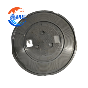
 The SiC Vacuum Chuck for Wafer Bonding is a high-performance precision ceramic adsorption component designed for advanced semiconductor packaging and wafer bonding applications.
Manufactured using high-purity CVD Silicon Carbide (SiC) or advanced sintered SiC technologies, this vacuum chuck provides exceptional thermal stability, ultra-high rigidity, and sub-micron-level surface precision for critical bonding processes.
Through precision vacuum adsorption structures and ultra-flat surface processing, the chuck securely holds wafers during wafer-to-wafer (W2W), chip-to-wafer (C2W), hybrid bonding, MEMS packaging, and advanced semiconductor assembly operations.
Its low thermal expansion and superior dimensional stability ensure accurate wafer positioning while minimizing thermal deformation during elevated-temperature processes.
Key Features
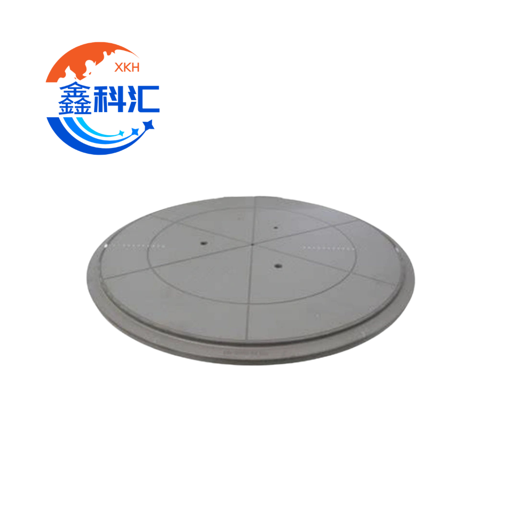
Ultra-Flat Wafer Adsorption Surface
- Surface flatness ≤ 1 μm
- Parallelism ≤ 1 μm
- Ensures highly uniform wafer contact
- Improves bonding alignment accuracy
Mirror-grade flatness minimizes local stress and reduces wafer deformation during bonding.
 Ultra-Smooth Mirror Polishing
Surface roughness:
Ra ≤ 0.01 μm
Benefits:
- Reduced particle contamination
- Improved vacuum sealing performance
- Stable wafer adsorption
- Semiconductor cleanroom compatibility
Exceptional Thermal Stability
Silicon carbide exhibits:
- Low thermal expansion coefficient (~4.5×10⁻⁶/°C)
- High thermal conductivity
- Excellent dimensional stability
This allows the chuck to maintain precise positioning under elevated-temperature bonding conditions.
High Mechanical Rigidity
Elastic modulus:
>400 GPa
Advantages:
- Prevents deformation under pressure
- Supports high wafer loading accuracy
- Improves process consistency
High stiffness is critical for sub-micron alignment processes.
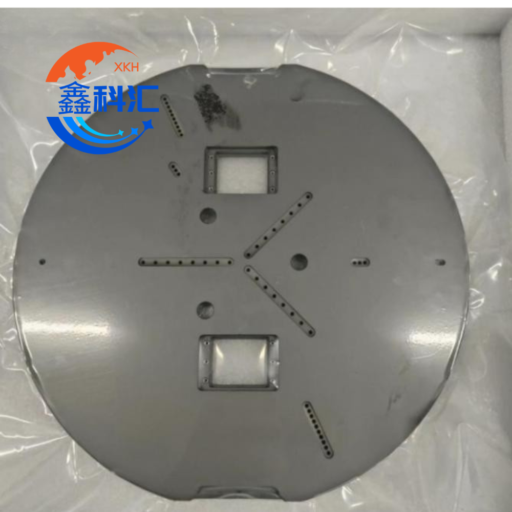
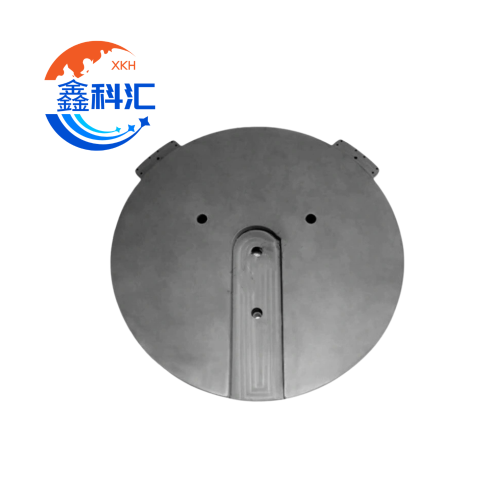
Precision Vacuum Channel Design
High-precision vacuum groove machining:
Accuracy:
±5 μm
Ensures:
- Uniform adsorption force distribution
- Stable wafer fixation
- Reduced local stress concentration
Technical Specifications
| Item | Specification |
|---|---|
| Material | High Purity Silicon Carbide |
| SiC Purity | ≥99.999% |
| Surface Flatness | ≤1 μm |
| Surface Roughness | Ra ≤0.01 μm |
| Elastic Modulus | >400 GPa |
| Thermal Conductivity | ~120 W/m·K |
| Density | ≥3.1 g/cm³ |
| CTE | ~4.5×10⁻⁶/°C |
| Groove Accuracy | ±5 μm |
| Operating Temperature | RT–400°C |
| Surface Treatment | Mirror Polished |
| Wafer Size | Custom Available |
Applications
Advanced Semiconductor Packaging
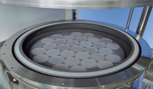 Widely used in:
- Wafer-to-Wafer (W2W) bonding
- Chip-to-Wafer (C2W) bonding
- Hybrid bonding
- Cu-Cu thermocompression processes
- 3D IC packaging
- System-in-Package (SiP)
MEMS Device Packaging
Provides stable wafer support for:
- Vacuum bonding
- Anodic bonding
- Sensor encapsulation
The rigid structure protects sensitive MEMS devices from thermal or mechanical distortion.
Power Semiconductor Devices
Suitable for:
- SiC module packaging
- GaN power device assembly
- Silver sintering
- TLP bonding
Excellent thermal stability ensures process consistency.
Photonics & Micro-LED Manufacturing
Supports:
- Micro-LED transfer systems
- Glass-silicon bonding
- Optical device integration
- Precision substrate positioning
Product Advantages
- Ultra-high purity SiC material
- Surface flatness ≤1 μm
- Mirror-polished adsorption surface
- Excellent thermal stability
- High stiffness and rigidity
- Low particle contamination
- Precision vacuum channel machining
- Suitable for advanced packaging environments
- Custom geometry available
Customization Options
We provide full OEM/ODM customization based on drawings or application requirements:
- Custom wafer diameters
- Vacuum groove layouts
- Through-hole structures
- Mirror polishing options
- Special adsorption zones
- Semiconductor-grade cleaning
- Ultra-flat processing
- Complex ceramic geometries
All products can be packaged in Class 100 cleanroom environments for semiconductor applications.
FAQ
Q1: Why use SiC instead of aluminum or quartz vacuum chucks?
SiC offers:
- Lower thermal expansion
- Higher rigidity
- Better temperature resistance
- Reduced contamination risk
- Longer operational life
Q2: Which bonding processes are supported?
Compatible with:
- W2W bonding
- C2W bonding
- Hybrid bonding
- Thermocompression bonding
- MEMS bonding
Q3: Can custom vacuum grooves be manufactured?
Yes. Groove patterns, hole layouts, adsorption areas, and dimensions can all be customized.
Q4: Is semiconductor-grade cleaning available?
Yes. Products can be cleaned and packaged in Class-100 cleanroom conditions.
Reviews
There are no reviews yet.