
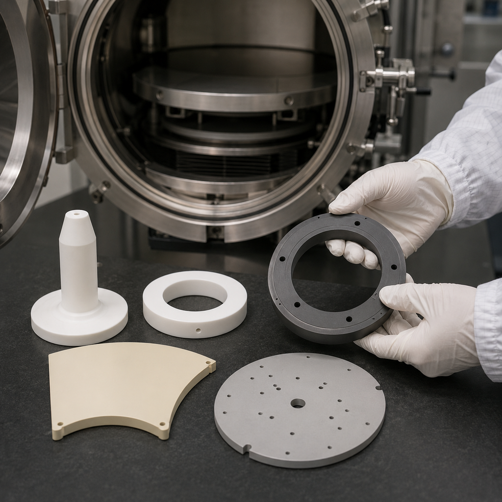
Semiconductor plasma etch chambers expose internal components to fluorine-, chlorine-, bromine- and oxygen-containing gases, energetic ions, ultraviolet radiation, vacuum and repeated thermal cycling.
Under these conditions, chamber hardware can gradually erode, change surface chemistry and release particles or metallic contaminants. Even a component that remains mechanically intact may become unsuitable if it alters process stability or increases wafer defect density.
Advanced ceramics such as alumina, yttria, aluminum nitride and silicon carbide are widely used because they combine high-temperature stability, dimensional accuracy and chemical resistance. However, no single ceramic is best for every chamber location.
Y₂O₃ generally provides strong resistance to fluorine-containing plasma, Al₂O₃ offers balanced performance and economical manufacturing, AlN combines electrical insulation with high thermal conductivity, and SiC provides high stiffness, thermal conductivity and semiconductor-compatible purity.
Correct selection requires matching the material to plasma chemistry, ion energy, component temperature, electrical function and acceptable contamination level.
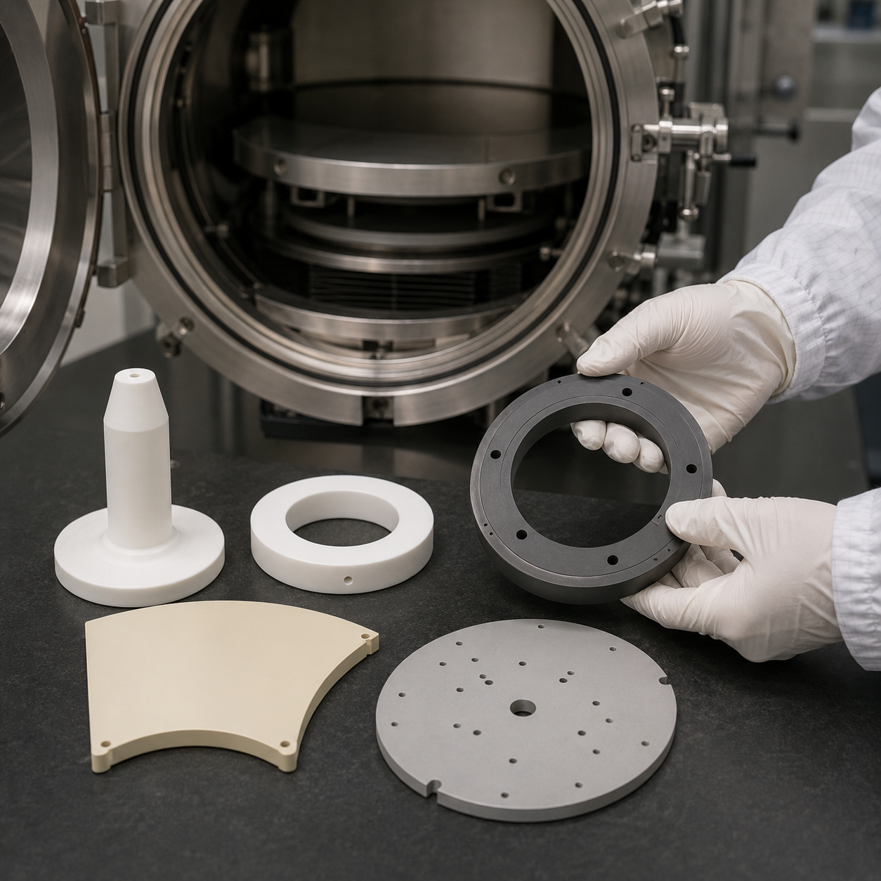
Why Etch-Chamber Materials Fail
Plasma erosion is not controlled by chemical corrosion alone. Material removal usually results from several mechanisms acting together.
Chemical Reaction
Reactive fluorine, chlorine or bromine species interact with the component surface and form new compounds. Depending on volatility and stability, these reaction products may remain as a protective layer or leave the surface as gas.
Physical Sputtering
Energetic ions strike the chamber component and physically remove atoms, grains or surface reaction products. Sputtering becomes particularly important near high-bias or direct line-of-sight plasma regions.
Preferential Grain-Boundary Attack
Polycrystalline ceramics contain grains, grain boundaries and sometimes residual pores. Plasma can attack these areas at different rates, producing a rough surface and eventually releasing grains as particles.
Thermal Stress
Rapid changes in temperature generate stress between the component surface and interior. Coatings can also experience stress because their coefficient of thermal expansion differs from the substrate.
Coating Delamination
A plasma-resistant coating can crack or detach when adhesion is inadequate, the substrate surface is poorly prepared or the coating contains excessive porosity and residual stress.
Process Deposits
Polymer, fluoride and metal-containing residues accumulate on chamber surfaces. These deposits can crack or flake during later process and cleaning cycles, even when the underlying ceramic has limited erosion.
For these reasons, material selection must consider the complete chamber process rather than only a published chemical-resistance table.
Plasma-Facing Components vs. Functional Components
A critical distinction is whether the ceramic is directly exposed to the highest plasma density.
Direct Plasma-Facing Components
Examples include:
- Focus rings
- Edge rings
- Chamber liners
- Gas nozzles
- Showerhead components
- Chamber domes
- Shields
- Insulating rings near the wafer
- Process-facing electrostatic chuck surfaces
For these parts, plasma erosion, particle generation and contamination are primary selection criteria.
Indirectly Exposed Functional Components
Examples include:
- Heater bodies
- Electrical insulators
- Support plates
- Feedthrough insulators
- Thermal-management components
- Structural spacers
- Backside ESC components
For these components, thermal conductivity, dielectric behavior, mechanical strength and dimensional stability may be more important than maximum direct plasma resistance.
This distinction explains why AlN can be an excellent heater or ESC material but may not be the first choice for an unprotected liner in an aggressive fluorine plasma.
Material Comparison
| Property | Al₂O₃ | Y₂O₃ | AlN | SiC |
|---|---|---|---|---|
| Main advantage | Balanced cost, insulation and manufacturability | Strong resistance to many fluorine plasmas | High thermal conductivity plus electrical insulation | High stiffness, hardness, thermal conductivity and purity |
| Typical thermal conductivity | Approximately 20–35 W/m·K | Approximately 10–15 W/m·K | Approximately 140–240 W/m·K | Approximately 80–200+ W/m·K |
| Electrical behavior | Insulating | Insulating | Insulating | Grade-dependent; semiconducting, conductive or semi-insulating |
| Direct fluorine-plasma resistance | Moderate to good, grade-dependent | Generally very good | Process- and grade-dependent | Process-dependent; fluorine can form volatile silicon species |
| Mechanical processing | Mature and cost-effective | More difficult and expensive | Precision grinding required | Difficult; diamond machining normally required |
| Common material forms | Dense bulk ceramic and coated substrates | Bulk ceramic, plasma-sprayed coating, aerosol-deposited coating | Dense bulk ceramic | Sintered SiC, reaction-bonded SiC and CVD SiC |
| Typical chamber applications | Nozzles, domes, insulators, liners and structural parts | Plasma-facing liners, shields, rings and protective coatings | ESCs, heaters, support plates and thermal components | Focus rings, edge rings, showerheads, susceptors and liners |
| Main limitation | Fluorination, roughening and particle generation under severe plasma | Cost, sintering difficulty and coating-related defects | Moisture sensitivity and chemical erosion in some direct plasma environments | Electrical behavior and volatile reaction products in some halogen plasmas |
The thermal conductivity values are approximate and vary with purity, porosity, grain structure and manufacturing method. Kyocera, for example, lists representative values of about 29 W/m·K for high-purity alumina, 14 W/m·K for yttria, 150 W/m·K for AlN and 200 W/m·K for one SiC grade. Kyocera ceramic thermal-conductivity comparison
Alumina Ceramic for Etch Chambers
Alumina is the most established technical ceramic and is commonly selected when a component needs a practical balance of plasma resistance, electrical insulation, mechanical strength and manufacturing cost.
Common grades include:
- 96% alumina
- 99% alumina
- 99.5% alumina
- 99.7% alumina
- 99.8% or 99.9% ultra-high-purity alumina
For chamber components, purity affects more than corrosion resistance. Lower-purity grades can contain glassy grain-boundary phases based on silicon, calcium, magnesium or alkali elements. Plasma exposure may preferentially attack these phases and release contaminants.
Morgan Technical Ceramics identifies high-purity and ultra-high-purity alumina for semiconductor processing, plasma environments and ultra-high vacuum applications. High-performance alumina ceramic components
Advantages of Alumina
- Mature forming and sintering processes
- Wide range of available component sizes
- Good electrical insulation
- Good dimensional stability
- Relatively high mechanical strength
- Easier sourcing than yttria or CVD SiC
- Suitable for complex precision-machined parts
- Lower cost than many specialized plasma-resistant materials
Alumina in Fluorine Plasma
Fluorine-containing plasma can react with Al₂O₃ and produce an aluminum fluoride-rich reaction layer. This layer may initially slow further chemical reaction, but energetic ion bombardment can remove it.
Continued cycling between fluorination and physical removal can lead to:
- Increased surface roughness
- Preferential grain-boundary erosion
- Aluminum-containing particles
- Changes in chamber conditioning
- Reduced component dimensions
- Process drift over extended use
Dense, high-purity alumina normally performs better than porous or lower-purity grades. Surface condition is also important because pores, machining damage and exposed grain boundaries can become erosion-initiation sites.
When to Select Alumina
Alumina is a strong starting choice for:
- General-purpose chamber insulators
- Gas-distribution nozzles
- Microwave introduction components
- Chamber domes
- Structural supports
- Vacuum feedthrough insulators
- Components with moderate plasma exposure
For severe, continuous fluorine-plasma exposure near the wafer, yttria or another rare-earth-based protective material may offer longer service life.
Yttria Ceramic for Fluorine-Plasma Resistance
Yttria is widely recognized for its resistance to fluorine-containing plasma and its ability to reduce particle and impurity contamination in semiconductor processing equipment. Kyocera’s yttria material overview specifically identifies plasma and corrosion resistance as its important properties.
When Y₂O₃ reacts with fluorine species, the surface can develop YF₃- and YOF-containing reaction products. These products are relatively stable and can reduce continued chemical material loss.
However, the reaction layer does not make yttria immune to erosion. High-energy ion bombardment can remove the fluoride layer and expose fresh Y₂O₃.
Advantages of Yttria
- Strong resistance to many fluorine-based plasma chemistries
- Lower erosion than alumina in many comparable fluorocarbon conditions
- Potential reduction in chamber-generated particles
- Good electrical insulation
- Suitable for plasma-facing rings, shields and liners
- Available as bulk ceramic or protective coating
Limitations of Yttria
- Higher raw-material and processing cost
- More difficult densification than alumina
- Lower thermal conductivity than AlN and SiC
- Brittle behavior in thin or mechanically loaded geometries
- Residual porosity can accelerate localized erosion
- Coating properties depend strongly on deposition process
- Yttrium contamination may be unacceptable for some device processes
Research on dense polycrystalline Y₂O₃ has shown that plasma behavior changes significantly with bias voltage, gas composition, porosity and crystal orientation. At high bias, physical sputtering can dominate even when the material has strong chemical resistance. Processing Map to Control the Erosion of Y₂O₃ in Fluorine-Based Etching Plasmas
This means “yttria is plasma-resistant” should never be interpreted as a fixed etch-rate guarantee.
Bulk Y₂O₃ vs. Y₂O₃ Coating
Yttria can be supplied as a dense bulk ceramic or as a coating applied to alumina, aluminum or another chamber substrate.
Bulk Yttria
Bulk yttria avoids coating-interface delamination and maintains the same nominal chemistry through the component thickness.
It may be preferred for:
- Small plasma-facing rings
- Nozzles
- Inserts
- Replaceable shields
- Components that will be repeatedly refinished
Its limitations include cost, sintering difficulty, machining risk and size restrictions.
Plasma-Sprayed Yttria Coating
Atmospheric plasma spraying can produce relatively thick protective layers on large chamber components. It is widely used for liners and shields.
Possible concerns include:
- Lamellar or splat microstructure
- Open and connected porosity
- Higher initial roughness
- Microcracks
- Nonuniform thickness around holes and edges
- Particle generation from weakly bonded regions
Aerosol-Deposited Yttria
Aerosol deposition can produce dense coatings at comparatively low substrate temperature. It may offer a finer and less porous structure than conventional plasma spraying.
Performance still depends on:
- Powder purity
- Particle size
- Substrate preparation
- Coating thickness
- Residual stress
- Surface finishing
Thin-Film Yttria
PVD, CVD, ALD and related methods can produce thinner and denser films. These are useful where contamination control and surface uniformity are more important than total sacrificial thickness.
No coating method should be selected by name alone. Porosity, adhesion, roughness, thickness uniformity and plasma test results are required.
Aluminum Nitride for Thermal and Electrical Functions
Aluminum nitride combines high thermal conductivity with electrical insulation. This makes it particularly valuable for components that must control wafer or chamber temperature while remaining electrically isolated.
Representative AlN grades can provide thermal conductivity of 150 W/m·K or higher, although the value depends strongly on oxygen concentration, sintering aids and microstructure. Kyocera’s AlN technical overview
Typical AlN Applications
- Electrostatic chuck bodies
- Ceramic heaters
- Thermal distribution plates
- RF and electrical insulation components
- High-power electrode supports
- Temperature-controlled wafer stages
- Backside chamber components
Advantages of AlN
- Much higher thermal conductivity than alumina or yttria
- Strong electrical insulation
- Coefficient of thermal expansion relatively close to silicon
- Good temperature uniformity
- Suitable for embedded heaters and electrodes
- Low particle generation when properly processed and finished
Limitations in Plasma Environments
AlN is not automatically the most durable choice for every directly exposed surface.
In fluorine-containing plasma, the surface may form aluminum fluoride species while nitrogen is removed. In chlorine-containing plasma, aluminum chloride-related reaction products may form under suitable conditions.
Potential consequences include:
- Surface roughening
- Changes in electrical properties
- Loss of nitrogen from the near-surface region
- Exposure of sintering additives
- Particle generation
- Reduced thermal uniformity after long service
AlN can also react with moisture, especially on damaged or unprotected surfaces. Cleaning and storage procedures should therefore be controlled.
AlN is strongest when selected for thermal-management and insulating functions, with direct high-density plasma exposure minimized or protected where necessary.
Silicon Carbide for Focus Rings and High-Purity Chamber Hardware
Silicon carbide combines high hardness, stiffness, thermal conductivity, heat resistance and dimensional stability.
It is frequently used for:
- Focus rings
- Edge rings
- Susceptors
- Showerhead components
- Chamber liners
- Wafer support components
- High-temperature process hardware
- Thermal management parts
SiC Grade Matters
The term “SiC ceramic” can describe very different materials.
Pressureless-Sintered SiC
Dense sintered SiC provides good strength, wear resistance and thermal properties. It may contain boron, carbon or other sintering additives.
Reaction-Bonded or Silicon-Infiltrated SiC
This material contains residual free silicon. Its chemical, electrical and plasma behavior can therefore differ from high-purity SiC.
CVD SiC
Chemical-vapor-deposited SiC can provide:
- Very high purity
- Dense, low-porosity structure
- Uniform microstructure
- Reduced metallic contamination
- Good surface-finish capability
CVD SiC is often preferred when high purity and contamination control justify the additional cost. Morgan notes that high-purity alumina and CVD SiC are used in plasma etch and other wafer-processing equipment because they can withstand repeated chemical and thermal cycles. Ceramic purity for semiconductor contamination control
SiC in Halogen Plasma
SiC is not chemically inert in every plasma.
Fluorine can react with silicon to form volatile SiF₄-related species. Chlorine chemistry can also remove silicon-containing material under suitable ion-energy and temperature conditions.
The carbon-rich surface left during selective silicon removal may change:
- Electrical impedance
- Surface roughness
- Polymer deposition
- Chamber seasoning
- Particle behavior
SiC performance therefore depends on plasma chemistry, conductivity grade, surface finish, grain structure and component location.
Electrical Properties
Unlike alumina, yttria and AlN, SiC is not automatically an electrical insulator.
Available grades may be:
- Electrically conductive
- Semiconducting
- High-resistivity
- Semi-insulating
For focus rings and RF-coupled chamber components, electrical resistivity can affect sheath behavior, plasma uniformity and etch profile. The required resistivity range should be specified rather than assuming all SiC behaves identically.
Material Selection by Plasma Chemistry
Fluorocarbon Plasma
Examples include CF₄, CHF₃, C₄F₈ and related mixtures.
Recommended considerations:
- Y₂O₃ is often favored for directly exposed liners and shields.
- High-purity Al₂O₃ is suitable for less severe areas or as a coated substrate.
- AlN is useful where heat transfer and insulation dominate, but direct exposure must be evaluated.
- SiC may erode through volatile silicon fluoride formation, although actual performance depends on ion energy and surface conditions.
NF₃ Chamber Cleaning
NF₃ generates reactive fluorine species and can be particularly demanding for chamber components.
Evaluate:
- Protective fluoride-layer stability
- Coating porosity
- Ion energy during cleaning
- Temperature
- Cleaning frequency
- Dimensional loss over repeated cycles
The material that performs well during the wafer etch recipe may still fail prematurely during chamber cleaning.
Chlorine and BCl₃ Plasma
Chlorine-containing plasma is used for etching metals, compound semiconductors and other materials.
Selection depends on whether the ceramic forms volatile chlorides and whether ion bombardment removes the resulting reaction layer.
High-purity alumina and selected SiC grades may be suitable, but testing under the actual Cl₂/BCl₃ ratio, bias and temperature is required.
HBr Plasma
HBr-based plasma is commonly used where highly controlled silicon etching and sidewall passivation are needed.
Bromine chemistry, polymer deposition and ion bombardment can create different surface responses from fluorocarbon plasma. Existing fluorine-plasma data should not be used as a direct substitute.
Oxygen and Argon Plasma
Oxygen plasma can oxidize SiC surfaces and alter carbon-containing residues. Argon mainly increases physical sputtering.
In an Ar-rich process, hardness, density, grain-boundary strength and coating adhesion may become more important than formation of a chemically protective fluoride layer.
Surface Finish and Particle Generation
A polished surface generally contains fewer exposed pores and machining defects, but the smoothest initial surface does not always remain the smoothest after plasma exposure.
Differential erosion can reveal:
- Grain boundaries
- Pores
- Secondary phases
- Coating splats
- Cracks
- Machining damage
The specification should define:
- Initial Ra or Sa surface roughness
- Measurement method and cutoff
- Maximum pores or pits
- Edge-chip limits
- Surface crack limits
- Post-cleaning surface condition
- Plasma-aged roughness limit, when critical
For coatings, three-dimensional areal roughness parameters may be more informative than a single line-based Ra value.
Purity and Sintering Additives
A high headline purity does not always guarantee low contamination.
The following should be separately controlled:
- Sodium
- Potassium
- Iron
- Nickel
- Chromium
- Calcium
- Magnesium
- Titanium
- Silicon
- Boron
- Carbon
- Rare-earth additives
Alumina may contain MgO, SiO₂, CaO or alkali-containing grain-boundary phases. AlN commonly uses Y₂O₃ or other additives to aid densification. Sintered SiC may contain boron and carbon, while reaction-bonded SiC contains free silicon.
Request a complete elemental analysis or certificate of analysis instead of relying only on “99.9% ceramic.”
How to Qualify a Plasma-Resistant Ceramic
Supplier datasheets should be used for initial screening, not final process qualification.
A useful plasma-exposure test should reproduce:
- Gas composition
- Gas flow
- Chamber pressure
- ICP or source power
- RF bias
- Ion energy
- Component temperature
- Exposure time
- Cleaning recipe
- Sample orientation
- Initial surface finish
Recommended post-test measurements include:
- Mass loss
- Step-height or thickness loss
- Surface profilometry
- SEM imaging
- EDS elemental analysis
- XPS surface chemistry
- XRD phase analysis
- Particle count
- Metallic contamination analysis
- Surface roughness
- Coating adhesion
Plasma erosion rates reported by different laboratories are often not directly comparable. Research on Y₂O₃ has shown that differences in reactor design, bias voltage, gas composition and material microstructure can produce significantly different conclusions.
The best comparison uses candidate materials tested side by side in the same equipment.
Component-Specific Selection Guide
| Component | Primary requirement | Common material direction |
|---|---|---|
| Focus or edge ring | Plasma stability, electrical behavior, dimensional accuracy | High-purity SiC, CVD SiC or process-qualified ceramic |
| Chamber liner | Low erosion and low particle generation | Y₂O₃ coating, bulk Y₂O₃ or high-purity Al₂O₃ |
| Gas nozzle | Purity, insulation and chemical resistance | High-purity Al₂O₃ or Y₂O₃ |
| Electrostatic chuck body | Thermal uniformity, insulation and plasma resistance | AlN or high-purity Al₂O₃ with application-specific surface protection |
| Ceramic heater | High thermal conductivity and electrical insulation | AlN |
| Chamber dome | Dielectric uniformity and plasma resistance | High-purity Al₂O₃, sapphire or specialized plasma-resistant ceramic |
| Susceptor | Thermal conductivity and dimensional stability | SiC or CVD-coated SiC |
| Protective shield | Low fluorine erosion and low contamination | Y₂O₃, YF₃, YOF or qualified rare-earth coating |
| Feedthrough insulator | Dielectric strength and vacuum reliability | High-purity Al₂O₃ |
| Showerhead component | Purity, gas distribution and plasma stability | SiC, CVD SiC, alumina or application-specific coated material |
RFQ Checklist
A ceramic chamber-component inquiry should include:
- Component name and installation location
- Direct or indirect plasma exposure
- Plasma gas composition
- Chamber-cleaning chemistry
- Source power and bias conditions
- Operating pressure
- Continuous and peak temperature
- Thermal-cycling frequency
- Required material and manufacturing route
- Minimum ceramic purity
- Maximum individual impurity limits
- Density and open porosity
- Grain-size or coating-microstructure requirements
- Electrical resistivity
- Dielectric constant and loss tangent
- Thermal conductivity
- Coefficient of thermal expansion
- Drawing with dimensional and geometric tolerances
- Surface-finish requirements
- Edge and chip criteria
- Cleaning and packaging method
- Certificate of analysis
- Dimensional inspection report
- Plasma-test data, if required
- Prototype and production quantities
Frequently Asked Questions
Is Y₂O₃ always better than Al₂O₃ in fluorine plasma?
Y₂O₃ often shows lower erosion in fluorine-containing plasma, but performance depends on density, porosity, surface finish, ion energy and coating quality. High-bias physical sputtering can still damage yttria.
Is AlN suitable for direct plasma exposure?
AlN can be used in plasma equipment, especially for heaters and electrostatic chucks. However, its main advantage is high thermal conductivity combined with electrical insulation. Direct exposure to aggressive halogen plasma must be qualified for the specific recipe.
Is CVD SiC better than sintered SiC?
CVD SiC normally offers higher purity and lower porosity, which can reduce contamination. Sintered SiC may provide lower cost and greater component-size flexibility. Plasma erosion and electrical behavior must still be evaluated.
Why do Y₂O₃ coatings generate particles?
Particle generation may result from coating porosity, weak splat boundaries, cracks, poor adhesion, uneven erosion or repeated thermal cycling. Nominal Y₂O₃ purity alone does not determine coating quality.
Can a published plasma etch rate be used to predict component life?
Only with caution. Etch rate depends strongly on reactor configuration, gas composition, pressure, source power, bias, temperature and sample microstructure. Side-by-side testing under the actual chamber conditions is more reliable.
Which ceramic has the highest thermal conductivity?
AlN and SiC generally have much higher thermal conductivity than alumina and yttria. The final selection must also consider electrical behavior, plasma chemistry, purity and mechanical design.
Conclusion
Selecting a plasma-resistant ceramic for a semiconductor etch chamber requires more than comparing material names.
Alumina provides a mature and cost-effective balance of insulation, strength and manufacturability. Yttria is especially valuable for plasma-facing surfaces exposed to fluorine chemistry, although coating porosity and high-energy sputtering remain important risks. Aluminum nitride is preferred where high thermal conductivity and electrical insulation are essential, while silicon carbide offers high stiffness, thermal performance and high-purity options for focus rings, susceptors and other critical chamber components.
The correct solution may combine materials—for example, an AlN heater body, an alumina structural insulator, a Y₂O₃-coated liner and a high-purity SiC focus ring.
Final qualification should be based on the actual plasma recipe, component position, thermal cycle, electrical function and acceptable particle level. A well-defined RFQ and controlled plasma-exposure test are more valuable than a generic claim that one ceramic is “plasma resistant.”

