
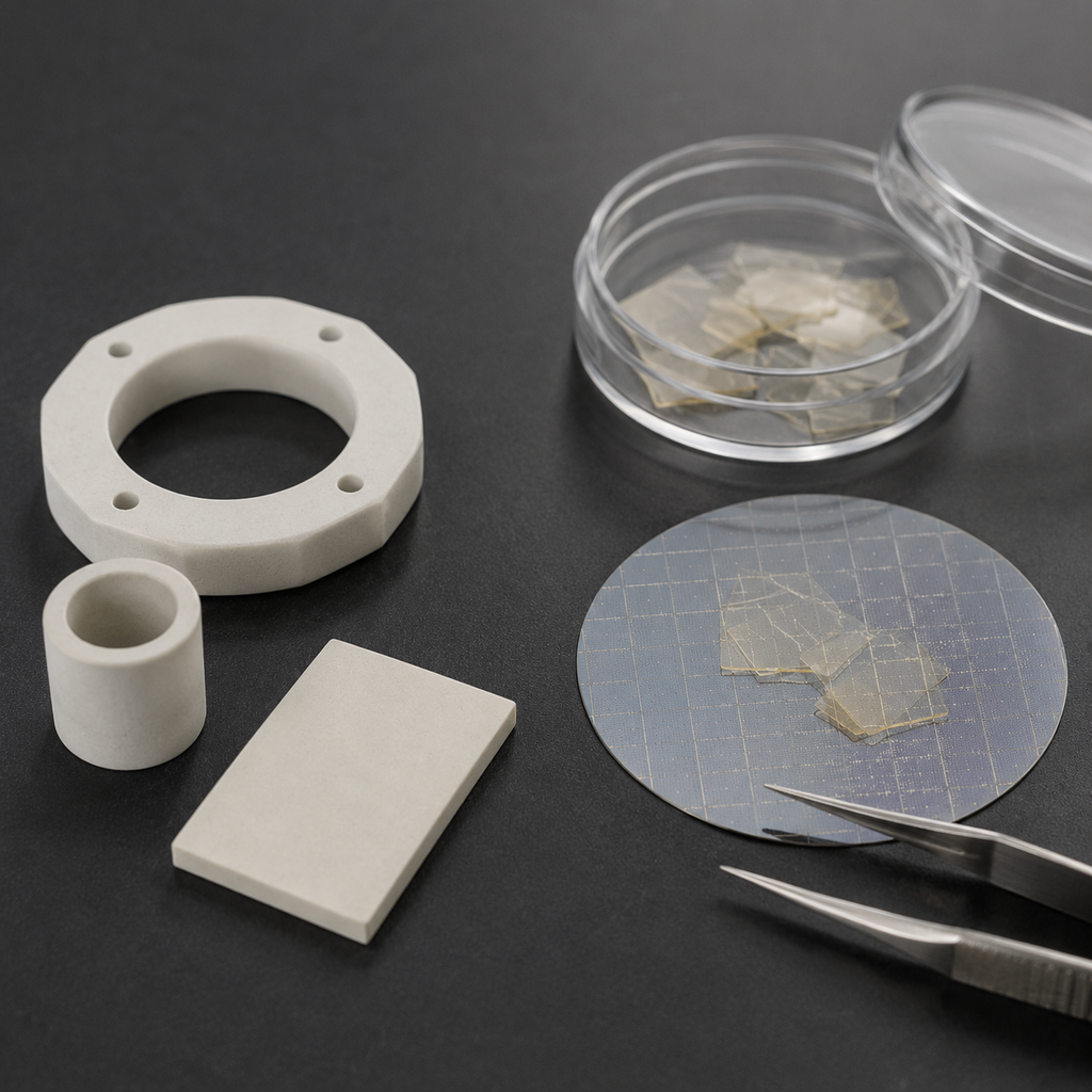
Hexagonal boron nitride appears in many semiconductor material catalogs, but the term “hBN” can describe products with very different structures and uses.
A machinable hBN ceramic component, a device-grade hBN single crystal, a pyrolytic boron nitride crucible and an hBN powder may all have the same basic chemical composition—boron and nitrogen—yet they cannot be used interchangeably.
Hot-pressed hBN ceramic is generally supplied as plates, rods, rings, sleeves, crucibles and custom-machined insulating components. Device-grade hBN single crystal is normally supplied as small layered crystals or exfoliable flakes for graphene, transition metal dichalcogenides and other two-dimensional device structures.
The correct material therefore depends on whether the application needs a three-dimensional ceramic component or an atomically flat crystalline interface.

What Is Hexagonal Boron Nitride?
Hexagonal boron nitride is a layered compound in which boron and nitrogen atoms form hexagonal sheets. Strong covalent bonds hold atoms together within each sheet, while comparatively weak van der Waals forces connect adjacent layers.
This structure is similar to graphite, which is why hBN is sometimes called “white graphite.” However, unlike graphite, conventional high-purity hBN is electrically insulating.
The layered structure gives hBN several important characteristics:
- High electrical resistivity
- Low dielectric loss
- High in-plane thermal conductivity
- Low friction and solid-lubricating behavior
- Good thermal shock resistance
- Chemical stability in many environments
- Weak bonding between adjacent crystal layers
It also creates strong anisotropy. Thermal conductivity, mechanical strength, electrical behavior and thermal expansion can differ substantially between directions parallel and perpendicular to the basal planes.
This anisotropy is important for both hot-pressed ceramic components and hBN single crystals.
What Is HBN Ceramic?
HBN ceramic is a bulk polycrystalline material manufactured from boron nitride powder. The powder is consolidated using hot pressing, pressure-assisted sintering or another densification process.
Commercial hBN ceramic may be:
- High-purity binderless hBN
- hBN containing a boric oxide binder
- hBN containing calcium borate
- hBN combined with silica
- hBN combined with aluminum nitride
- hBN combined with silicon nitride
- hBN combined with zirconia or other reinforcing phases
These additions change density, strength, moisture resistance, oxidation behavior, thermal conductivity, dielectric properties and machinability.
Momentive describes hot-pressed BN solids as readily machinable materials produced by sintering at high temperature and pressure. Its material portfolio includes binderless grades and composites designed for different requirements. Momentive’s boron nitride solids guide also identifies semiconductor equipment insulators, evaporation crucibles and high-temperature components as typical applications.
Typical Forms of HBN Ceramic
HBN ceramic is commonly supplied as:
- Machinable plates and blocks
- Round rods and tubes
- Electrical insulating rings
- Furnace fixtures
- Crucibles
- Nozzles
- Sleeves
- Bushings
- Support components
- Custom precision-machined parts
It is selected when the customer needs a physical component with a defined shape, mounting features, dimensions and tolerances.
What Is HBN Single Crystal?
HBN single crystal consists of a continuous, highly ordered crystalline lattice rather than a consolidated mass of many powder particles.
High-quality bulk hBN single crystals can be grown using high-pressure, high-temperature methods. Other methods include flux growth, atmospheric-pressure growth and vapor-phase processes. The growth method affects crystal size, impurity level, defect density, color, optical properties and exfoliation quality.
Device-grade crystals are typically used as a source of thin flakes. Individual layers or multilayer flakes can be mechanically exfoliated and transferred into two-dimensional heterostructures.
The single crystal is not normally purchased to make a large mechanical component. Its value lies in its crystalline quality, atomically smooth basal surface, low defect density and ability to form clean interfaces with other two-dimensional materials.
NIMS researchers have demonstrated that high-purity hBN single crystals provide an exceptionally flat and electrically insulating substrate for graphene and other atomic-layer materials. According to NIMS’s semiconductor materials research overview, an hBN single-crystal substrate can reduce surface potential fluctuations compared with conventional SiO₂ surfaces.
Research on graphene devices has also shown enhanced mobility, reduced carrier inhomogeneity and lower intrinsic doping when graphene is placed on single-crystal hBN rather than SiO₂. These results helped establish hBN as an essential platform for high-quality two-dimensional electronics. Boron Nitride Substrates for High-Quality Graphene Electronics
HBN Ceramic vs. HBN Single Crystal
| Property | HBN ceramic | HBN single crystal |
|---|---|---|
| Basic structure | Polycrystalline hot-pressed or sintered body | Continuous ordered crystal lattice |
| Starting material | hBN powder, with or without binders and additives | Crystal grown from controlled high-purity source materials |
| Typical form | Plate, rod, ring, sleeve, crucible or custom part | Small platelet, flake or layered bulk crystal |
| Primary function | Electrical insulation, thermal management and high-temperature structural component | Substrate, dielectric layer or encapsulation material for electronic and quantum devices |
| Machinability | Can be conventionally machined using suitable tools | Normally cleaved, exfoliated and transferred rather than conventionally machined |
| Surface | Machined polycrystalline surface | Atomically flat basal crystal plane |
| Thermal behavior | Strongly affected by porosity, additives and pressing direction | Intrinsically anisotropic and highly dependent on crystal direction |
| Purity definition | Total hBN content plus binder and trace impurities | Crystal impurity concentration, defect density and optical/electronic quality |
| Typical size | Millimeter- to hundreds-of-millimeters-scale components | Usually much smaller crystals or flakes |
| Mechanical use | Suitable for low-load insulating and high-temperature components | Not intended as a conventional mechanical wear part |
| Semiconductor role | Equipment hardware and process components | Direct contact with active two-dimensional device layers |
| Cost basis | Material grade, component dimensions and machining complexity | Crystal size, purity, defect density and exfoliation quality |
Why HBN Ceramic Is Machinable
Unlike alumina, silicon carbide and silicon nitride, hot-pressed hBN is relatively soft and has a graphite-like layered structure. Cutting forces can separate the plate-like grains instead of requiring extensive diamond grinding.
Depending on the grade, hBN ceramic can be machined using:
- Carbide tools
- Diamond-coated tools
- Conventional turning
- Milling
- Drilling
- Grinding
- Saw cutting
The preferred tool depends on hBN purity, binder system, reinforcement phase and required surface quality.
Pure or high-hBN-content grades are generally easier to machine than composites containing hard phases such as zirconia, silicon carbide or aluminum nitride. However, high-purity binderless hBN may have lower mechanical strength and more fragile edges.
Machining Precautions
A machinable material is not the same as a damage-proof material. HBN ceramic can chip, delaminate or crack if it is clamped or machined incorrectly.
Recommended design and machining practices include:
- Use sharp cutting tools
- Apply light, controlled cutting loads
- Support thin walls during machining
- Avoid sharp internal corners
- Add suitable edge chamfers
- Avoid excessive clamping pressure
- Increase hole diameter gradually
- Avoid deep, narrow blind holes where possible
- Control dust with appropriate extraction equipment
- Confirm the preferred machining direction relative to the pressing direction
Very tight tolerances may still be possible, but they should be reviewed together with wall thickness, feature depth, material orientation and edge condition.
Can HBN Single Crystal Be Machined?
HBN single crystal is not normally machined into rings, sleeves or complex three-dimensional components.
The weak interlayer bonding that makes hBN useful for exfoliation also makes bulk crystals prone to cleavage. Conventional drilling or milling can split the crystal along the basal planes and introduce cracks or contamination.
Device fabrication normally uses processes such as:
- Mechanical exfoliation
- Deterministic dry transfer
- Wet transfer
- Layer stacking
- Plasma etching after transfer
- Electron-beam lithography
- Laser patterning for selected research structures
- Focused ion beam preparation for specialized analysis
When purchasing hBN single crystal, the customer should focus on crystal quality, lateral dimensions, thickness, impurity level, surface condition and exfoliation yield—not conventional machining tolerances.
Thermal Conductivity Is Direction-Dependent
One of the most common specification mistakes is requesting a single thermal conductivity value for hBN.
Because hBN has a layered crystal structure, heat moves much more efficiently along the basal planes than across them.
HBN Single Crystal Thermal Conductivity
High-quality hBN single crystals can have in-plane thermal conductivity in the hundreds of W/m·K at room temperature. Through-plane thermal conductivity is much lower because heat must move across the weakly bonded layers.
Experimental and theoretical studies confirm that bulk hBN has strongly anisotropic thermal transport. The difference is influenced by temperature, isotope composition, defect concentration, sample thickness and measurement method. Anisotropic Thermal Transport in Bulk Hexagonal Boron Nitride
This means a thin hBN layer may spread heat effectively across the device plane while offering much less efficient heat transfer through its thickness.
HBN Ceramic Thermal Conductivity
Hot pressing tends to align hBN platelets. The thermal conductivity of a ceramic block therefore depends on:
- Pressing direction
- Basal-plane orientation
- Density
- Porosity
- hBN purity
- Binder content
- Reinforcing additives
- Test temperature
A high-purity, highly oriented hBN ceramic can have significantly better thermal conductivity in one direction than another. A composite grade may sacrifice thermal conductivity to gain strength, moisture resistance or wear resistance.
A ceramic supplier should report thermal conductivity in relation to the pressing direction, for example:
- Parallel to the hot-pressing direction
- Perpendicular to the hot-pressing direction
However, manufacturers do not always use identical directional terminology. A drawing should therefore include a physical orientation diagram instead of relying only on “parallel” and “perpendicular.”
Thermal Contact Resistance
High intrinsic thermal conductivity does not guarantee efficient heat removal from an assembled device.
Actual thermal performance also depends on:
- Surface flatness
- Surface roughness
- Contact pressure
- Interfacial gaps
- Joining material
- Component thickness
- Heat-flow direction
- Thermal expansion mismatch
For thermal-management applications, the assembled interface should be evaluated rather than selecting a material using conductivity alone.
Electrical and Dielectric Performance
Both hBN ceramic and hBN single crystal are generally electrical insulators, but their electrical specifications serve different purposes.
HBN Ceramic
Machinable hBN ceramic can be used for:
- High-temperature electrical insulation
- Furnace insulators
- Semiconductor processing equipment insulators
- Plasma system components
- Microwave and RF insulation
- Heat-spreading electrical isolation
Relevant specifications include:
- Volume resistivity
- Dielectric strength
- Dielectric constant
- Dissipation factor
- Test frequency
- Test temperature
- Measurement direction
- Moisture conditioning
Not every BN composite is insulating. For example, BN-TiB₂ composites may be intentionally electrically conductive. The full grade composition must therefore be reviewed.
HBN Single Crystal
Device-grade hBN single crystal is valued as a wide-bandgap dielectric and encapsulation layer. It can electrically isolate graphene or another 2D semiconductor while maintaining an atomically smooth interface.
Important device properties include:
- Low surface roughness
- Low trap density
- Low impurity concentration
- High breakdown field
- Controlled thickness
- Clean transfer behavior
- Low interfacial contamination
- Low defect density
The dielectric behavior of a thin hBN flake should not be assumed from a bulk ceramic datasheet.
Purity and Binder Systems in HBN Ceramic
“High-purity hBN ceramic” should not be specified using the BN percentage alone.
Commercial machinable grades may contain binders or reinforcing phases designed to improve particular properties.
Binderless High-Purity HBN
Binderless grades provide:
- Higher hBN purity
- Better high-temperature performance in inert gas or vacuum
- Lower risk of binder contamination
- Good thermal conductivity
- Strong electrical insulation
Possible disadvantages include lower mechanical strength, fragile edges and sensitivity to machining orientation.
Saint-Gobain lists a binderless hBN grade with more than 99.7% purity and service capability above 2,000°C in inert or vacuum environments. This temperature should not be treated as an air-service rating. Saint-Gobain BN Machinable Ceramics
Boric Oxide-Bonded HBN
B₂O₃-containing grades can offer improved density and mechanical strength. However, boric oxide is hygroscopic, so exposure to moisture may change dimensional or electrical performance.
Storage, drying and moisture conditioning should be defined where relevant.
Calcium Borate-Bonded HBN
Calcium borate systems can provide improved moisture resistance compared with traditional boric oxide-bonded grades. They are often used where machinability and thermal shock resistance are both required.
HBN Composite Ceramics
HBN may be combined with materials such as SiO₂, AlN, Si₃N₄, ZrO₂ or SiC.
Composite grades can improve:
- Mechanical strength
- Moisture resistance
- Erosion resistance
- Wear resistance
- Thermal shock resistance
- Dimensional stability
The tradeoff may include lower hBN purity, reduced machinability or changed thermal and dielectric performance.
Temperature Limits Depend on Atmosphere
It is misleading to specify only a maximum temperature without defining the operating atmosphere.
HBN can maintain performance at very high temperatures in:
- Vacuum
- Nitrogen
- Argon
- Other suitable inert atmospheres
Its allowable temperature is much lower in oxidizing atmospheres. Oxidation can produce boron oxide, change the surface condition and gradually consume the component.
The customer should specify:
- Maximum continuous temperature
- Peak temperature
- Heating and cooling rate
- Vacuum level or gas composition
- Oxygen and moisture content
- Expected exposure time
- Contact materials
- Whether the part experiences thermal cycling
A high vacuum temperature rating should never be used as an air-service rating.
Semiconductor Applications of HBN Ceramic
Machinable hBN ceramic is primarily an equipment material rather than an active semiconductor substrate.
Typical applications include:
High-Temperature Electrical Insulators
HBN ceramic can electrically isolate heaters, electrodes, power feedthroughs and structural elements while tolerating rapid temperature changes.
Metal Evaporation Crucibles
Its non-wetting behavior and resistance to many molten materials make hBN suitable for selected evaporation and metal-processing applications.
Compatibility must still be confirmed for the exact source material, temperature and atmosphere.
Vacuum and Furnace Components
HBN ceramic can be used for:
- Furnace supports
- Insulating spacers
- Heater fixtures
- Thermocouple supports
- Vacuum processing components
- High-temperature sample holders
Plasma Equipment Components
Selected hBN grades are used in plasma-related systems because of their electrical insulation and thermal shock resistance. Performance depends on plasma chemistry, ion energy, temperature and binder composition.
HBN should not automatically be considered the best material for every fluorine- or chlorine-based semiconductor plasma. Plasma erosion, contamination and particle generation must be tested under actual process conditions.
Compound Semiconductor Processing
HBN ceramic may be used for insulating, supporting or containment components in equipment for processing GaN, SiC and other compound semiconductor materials.
The ceramic generally does not replace the active wafer substrate. It supports the equipment environment around the wafer or source material.
Semiconductor Applications of HBN Single Crystal
HBN single crystal serves a fundamentally different role.
Graphene Substrates
The atomically flat hBN surface reduces substrate-induced disorder compared with conventional amorphous oxide surfaces. This enables higher-quality graphene transport measurements and device structures.
Encapsulation of Two-Dimensional Materials
A graphene or TMD layer can be enclosed between upper and lower hBN flakes. Encapsulation protects the active material from contamination and environmental degradation.
Gate Dielectric Layers
Thin hBN flakes can function as dielectric barriers in field-effect transistors and tunneling structures.
Van der Waals Heterostructures
HBN can be stacked with:
- Graphene
- MoS₂
- WS₂
- WSe₂
- Black phosphorus
- Other layered materials
The absence of conventional dangling bonds supports clean interfaces without requiring traditional lattice-matched epitaxy.
Moiré and Quantum Devices
Rotational alignment between graphene and hBN can create a moiré superlattice. These structures are used to investigate quantum Hall physics, correlated electronic behavior and engineered band structures.
Deep-Ultraviolet Research
High-quality hBN single crystals have also been studied for deep-ultraviolet emission because of their wide bandgap and excitonic properties.
HBN Ceramic Is Not the Same as Pyrolytic Boron Nitride
Pyrolytic boron nitride, commonly abbreviated PBN, is another material that should not be confused with hot-pressed hBN ceramic or hBN single crystal.
PBN is generally deposited through a chemical vapor deposition process. It can provide:
- Very high purity
- Low porosity
- Strong anisotropy
- Smooth deposited surfaces
- Complex crucible and coating geometries
PBN is widely used for semiconductor crystal-growth crucibles, evaporation systems and high-purity furnace components.
The distinction can be summarized as follows:
- Hot-pressed hBN ceramic is powder-based and machinable.
- PBN is vapor-deposited and normally supplied as a deposited shape or coating.
- HBN single crystal is grown for crystallographic and electronic quality.
How to Specify HBN Ceramic
An RFQ for an hBN ceramic component should include:
- Required hBN grade
- Minimum BN content
- Binder or additive composition
- Maximum trace impurity limits
- Bulk density
- Open porosity, if critical
- Pressing direction and component orientation
- Thermal conductivity in each required direction
- Electrical resistivity
- Dielectric strength
- Dielectric constant and test frequency
- Maximum temperature and operating atmosphere
- Moisture resistance
- Outgassing requirements
- Component dimensions
- Dimensional and geometric tolerances
- Surface finish
- Edge chamfer requirements
- Cleaning method
- Packaging requirements
- Inspection report requirements
- Prototype and production quantities
If semiconductor cleanliness is important, specify individual limits for elements such as sodium, iron, calcium, silicon, aluminum and transition metals rather than relying only on total BN purity.
How to Specify HBN Single Crystal
A device-grade hBN single-crystal RFQ should include:
- Crystal growth method, if required
- Natural or controlled boron isotope composition
- Minimum lateral crystal size
- Crystal thickness range
- Required exfoliable area
- Number of crystals or total mass
- Color and transparency requirements
- Maximum impurity concentration
- Defect-density requirements
- Surface contamination limits
- Raman characterization requirements
- X-ray diffraction data, if required
- Cathodoluminescence or photoluminescence data
- AFM surface-roughness data
- Exfoliation-yield expectation
- Storage atmosphere
- Handling and packaging method
For 2D device research, the largest visible crystal is not necessarily the best crystal. Low defect density, clean exfoliation, uniform optical response and low interfacial contamination may be more important than overall crystal dimensions.
Which HBN Material Should You Select?
Choose machinable hBN ceramic when the application requires:
- A three-dimensional insulating component
- A crucible, ring, plate, sleeve or support
- Conventional machining
- High-temperature dimensional stability
- Thermal shock resistance
- Electrical insulation combined with heat spreading
Choose hBN single crystal when the application requires:
- An atomically flat substrate
- Graphene or TMD encapsulation
- A van der Waals heterostructure
- A thin dielectric barrier
- Moiré device fabrication
- Quantum transport research
Choose PBN when the application requires:
- A vapor-deposited high-purity crucible
- Low-porosity furnace hardware
- A deposited BN coating
- High-purity semiconductor source containment
Choose hBN powder when the application requires:
- A thermally conductive filler
- A release coating
- A lubricant additive
- A precursor for ceramic processing
Frequently Asked Questions
Is HBN ceramic made from HBN single crystals?
HBN ceramic is manufactured from many powder particles that are consolidated into a polycrystalline body. It does not have the continuous crystal lattice or atomically uniform surface of a device-grade single crystal.
Can HBN single crystal be used as a machinable ceramic plate?
Normally no. Single crystals are relatively small, layered and prone to cleavage. They are selected for their electronic interface quality rather than conventional mechanical machining.
Does HBN ceramic have high thermal conductivity?
It can, but the value depends strongly on material orientation, density, binder content and measurement direction. Both parallel and perpendicular conductivity values should be requested.
Can HBN ceramic operate above 2,000°C?
Some high-purity binderless grades can operate above 2,000°C in suitable inert or vacuum environments. Their allowable temperature in air is much lower. The atmosphere must always be included in the specification.
Which form of HBN is best for graphene devices?
High-quality hBN single crystal is normally required for graphene substrates and encapsulation. A machined polycrystalline hBN ceramic surface does not provide the same atomically flat and low-disorder interface.
Is the highest-purity HBN ceramic always the best choice?
No. A binderless grade may provide higher purity and temperature capability, while a binder-containing or composite grade may offer better strength, moisture resistance or wear performance. Grade selection must follow the application.
Conclusion
HBN ceramic and hBN single crystal share the same basic hexagonal boron nitride chemistry, but they serve completely different engineering purposes.
HBN ceramic is a bulk, polycrystalline, machinable material used for electrical insulation, high-temperature fixtures, crucibles and semiconductor equipment components. Its performance depends on density, binder composition, platelet orientation, porosity and machining quality.
HBN single crystal is a high-value electronic and research material selected for its atomically flat surface, low defect density and ability to form clean van der Waals interfaces with graphene and other two-dimensional materials.
A correct specification should therefore begin with the application. If the requirement is a machined component, specify the ceramic grade, binder, orientation, dimensions and operating atmosphere. If the requirement is a device interface, specify crystal growth quality, size, thickness, defect level and characterization data.
Treating these two forms of hBN as interchangeable can result in incorrect thermal calculations, unsuitable machining requirements, device contamination or failure to achieve the required electronic performance.

