
As semiconductor devices move toward more complex three-dimensional structures, deposition processes must create increasingly uniform films across deep trenches, narrow gaps and large wafer surfaces. Atomic layer deposition (ALD) and chemical vapor deposition (CVD) therefore depend not only on precursor chemistry and chamber design, but also on precise wafer temperature control.
For 300mm processing equipment, the heater pedestal is a critical part of this thermal system. It must support the wafer, distribute heat uniformly, maintain dimensional stability, electrically isolate embedded circuits and operate reliably under vacuum, reactive gases and repeated chamber-cleaning cycles.
Aluminum nitride, commonly abbreviated as AlN, is frequently selected for advanced ceramic heater pedestals because it combines relatively high thermal conductivity with electrical insulation and a coefficient of thermal expansion reasonably close to silicon. However, choosing AlN alone does not guarantee good temperature uniformity or long service life. Heater-zone layout, resistance stability, ceramic purity, hot-state flatness, shaft joining and process compatibility must be engineered as one system.
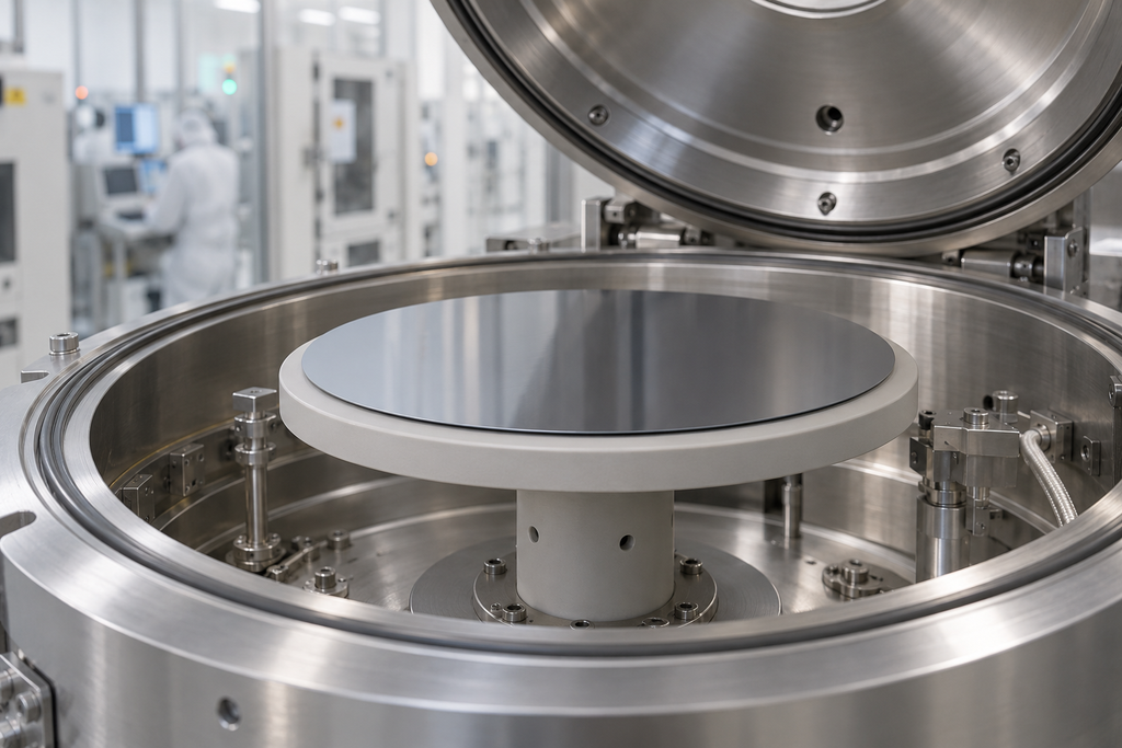
What Is an AlN Ceramic Heater Pedestal?
An AlN ceramic heater pedestal is a wafer-support and heating assembly used inside semiconductor process chambers. A typical design may include:
- A circular aluminum nitride ceramic plate
- One or more embedded resistance-heating circuits
- Electrical terminals or internal conductors
- Temperature sensors
- A ceramic or metal support shaft
- Vacuum-compatible plate-to-shaft joints
- Optional RF electrodes
- Optional electrostatic chucking electrodes
- Optional backside gas or purge channels
- Precision-ground wafer-contact surfaces
The pedestal supports the wafer at a controlled height and temperature while process gases flow around or above it. Depending on the equipment design, it may function only as a heater, or it may combine heating, wafer chucking, RF coupling, gas distribution and temperature sensing.
Commercial semiconductor heater designs demonstrate that resistance-heating elements and RF electrodes can be co-sintered within an AlN ceramic plate. Some designs directly join the ceramic shaft to the heater plate to create a compact assembly. These features are described in public product information from NGK Insulators and CoorsTek.
Why ALD and CVD Processes Require Precise Pedestal Heating
Wafer temperature influences several important deposition results:
- Film growth rate
- Surface reaction completion
- Precursor adsorption and desorption
- Film density
- Chemical composition
- Crystallinity
- Residual stress
- Step coverage
- Within-wafer thickness uniformity
- Wafer-to-wafer repeatability
ALD depends on sequential, self-limiting surface reactions. Each process has a temperature range in which the intended surface reactions operate correctly. Temperatures outside this range may cause incomplete reactions, precursor condensation or unwanted thermal decomposition.
CVD processes can involve continuous gas-phase and surface reactions at elevated temperatures. Local temperature differences can change reaction rates and produce center-to-edge variations in film thickness or material properties.
Advanced memory structures make these requirements more demanding. Lam Research has noted that current DRAM scaling increasingly relies on highly conformal ALD processes for gap fill, spacers and barrier layers in high-aspect-ratio structures. Its 2026 technology discussion illustrates how deposition precision is becoming more important as memory architectures grow more complex. Lam Research
Why Aluminum Nitride Is Used
High Thermal Conductivity
Dense aluminum nitride transfers heat much more effectively than conventional alumina ceramics. This helps spread heat from the embedded circuit through the ceramic plate and reduces localized hot spots.
Published values vary considerably by grade. Commercial AlN ceramics can have room-temperature thermal conductivity ranging from approximately 80 W/m·K to more than 200 W/m·K. Oxygen content, porosity, grain structure, sintering additives and secondary phases all affect the final value.
For example, public data from different manufacturers show AlN grades with different thermal conductivity values rather than one universal specification. Kyocera lists AlN as a high-conductivity electrically insulating ceramic, while NGK publishes different conductivity values for different AlN electrostatic chuck grades.
Consequently, an RFQ should specify the minimum acceptable thermal conductivity and measurement temperature instead of requesting only “high-purity AlN.”
Electrical Insulation
The ceramic body must electrically isolate the resistance heater from the wafer, chamber and mounting structure. AlN provides this insulation while still transferring heat efficiently.
Electrical behavior nevertheless depends on material formulation and temperature. Volume resistivity measured at room temperature may differ significantly from resistivity at the process setpoint. Some AlN grades are intentionally engineered with controlled resistivity for Johnsen–Rahbek electrostatic chucking, while heater-grade materials may prioritize high electrical insulation.
The specification should therefore state:
- Minimum volume resistivity
- Test temperature
- Test atmosphere
- Dielectric strength
- Maximum operating voltage
- Allowable leakage current
A room-temperature resistivity value alone is insufficient for a high-temperature heater pedestal.
Thermal Expansion Close to Silicon
Typical dense AlN grades have a coefficient of thermal expansion of approximately 4.5–5.7 × 10⁻⁶/K, depending on grade and test range. This is closer to silicon than conventional alumina and can help reduce differential expansion between the wafer and pedestal.
Kyocera lists a representative AlN CTE of approximately 4.6 × 10⁻⁶/K between 40°C and 400°C, while also emphasizing that property values depend on the selected material grade. Kyocera ceramic property data
The benefit is important, but CTE matching must also include:
- Embedded metal circuits
- Electrical terminals
- Plate-to-shaft joints
- Brazed interfaces
- Mounting hardware
- Any applied coating
A well-matched ceramic plate can still fail if an attached metal or joint introduces excessive thermal stress.
Why 300mm Heater Pedestals Are More Difficult
A 300mm wafer has 2.25 times the surface area of a 200mm wafer. The larger heated area increases the difficulty of maintaining uniform temperature, flatness and mechanical stability.
Common 300mm challenges include:
- Greater center-to-edge heat-loss differences
- Increased sensitivity to heater-pattern errors
- Larger accumulated dimensional change during heating
- Greater potential for plate deflection
- More difficult edge-zone temperature control
- Higher total electrical power
- Greater stress around the shaft connection
- Longer heating and cooling response times
- More demanding wafer-loading and edge-clearance requirements
Scaling a successful 200mm heater pattern to a larger diameter does not automatically produce a successful 300mm pedestal. The heater circuit, plate thickness, zone arrangement, thermal insulation, shaft geometry and control algorithm normally require separate optimization.
Temperature Uniformity Is a System Specification
High AlN thermal conductivity improves lateral heat spreading, but it does not guarantee uniform wafer temperature by itself.
Actual temperature distribution depends on:
- Heater-trace geometry
- Electrical power density
- Number of independently controlled zones
- Pedestal thickness
- AlN thermal conductivity
- Chamber-wall temperature
- Gas pressure and composition
- Wafer-to-pedestal contact
- Backside gas conditions
- Edge radiation and convection losses
- Shaft heat loss
- Sensor position
- Control-system response
Heater-Zone Design
A single-zone heater may be suitable when process conditions and uniformity requirements are moderate. More demanding equipment may use multiple concentric or independently controlled zones.
Typical zones may include:
- Center zone
- Intermediate zone
- Outer or edge-compensation zone
- Special correction areas near terminals or structural features
The outer zone often requires different power density because the pedestal edge loses heat differently from its center. However, adding more zones also increases conductor complexity, control requirements and potential failure points.
The correct number of zones should be determined through thermal modeling and experimental temperature mapping.
Define What “Temperature Uniformity” Means
A specification such as “excellent temperature uniformity” cannot be inspected objectively. Buyers should define:
- Target setpoint
- Allowed center-to-edge variation
- Measurement radius
- Edge exclusion
- Chamber pressure
- Gas environment
- Installed or standalone condition
- Wafer present or absent
- Stabilization time
- Ramp or steady-state measurement
- Sensor and calibration method
Temperature uniformity measured on an exposed heater in air may not represent wafer temperature inside an operating vacuum chamber.
Some commercial AlN heater suppliers publish extremely tight uniformity examples for selected configurations. These results should be treated as product-specific examples, not as universal performance for every AlN heater.
Embedded Resistance-Heater Design
Embedded heating elements are commonly created from refractory conductive materials compatible with ceramic firing and long-term operating temperatures. Depending on the manufacturing route, candidate materials may include tungsten, molybdenum or proprietary refractory-metal compositions.
Important design factors include:
- Heater resistance at room temperature
- Resistance at operating temperature
- Temperature coefficient of resistance
- Maximum current and voltage
- Local current density
- Trace width and thickness
- Distance from the wafer-support surface
- Electrical insulation thickness
- Zone-to-zone isolation
- Terminal geometry
- CTE compatibility with AlN
- Resistance stability after thermal cycling
Why Trace Geometry Matters
The embedded circuit determines where heat is generated. Incorrect trace spacing or abrupt changes in conductor geometry can create local power-density differences.
Potential consequences include:
- Hot spots
- Cold regions
- Local ceramic stress
- Heater resistance drift
- Film non-uniformity
- Premature conductor failure
The design must compensate for edge losses, shaft conduction and terminal areas. Finite-element thermal analysis can reduce development risk, but a simulation must use realistic boundary conditions and verified material properties.
Embedded RF or Chucking Electrodes
Some heater pedestals also incorporate:
- RF bias electrodes
- Ground electrodes
- Electrostatic chuck electrodes
- Backside gas channels
- Wafer-presence sensing structures
Combining these functions can reduce chamber complexity, but it makes the internal ceramic architecture more demanding. The heater and RF systems must avoid unwanted electrical coupling, arcing, localized heating and dielectric breakdown.
When an integrated pedestal is required, the RF frequency, voltage, power, grounding arrangement and intended chucking mechanism must be supplied during the design stage.
Flatness Requirements
Pedestal flatness affects wafer contact, heat transfer, chucking behavior and film uniformity. However, “flatness” can describe several different conditions.
A complete specification should distinguish among:
Cold-State Flatness
Measured at room temperature before installation. This is useful for incoming inspection but does not show how the pedestal behaves at process temperature.
Hot-State Flatness
Measured or predicted at the specified operating temperature. Thermal gradients, material expansion and internal circuit stresses may change the surface profile.
Installed Flatness
Measured after the pedestal is connected to its shaft, mounting structure and chamber. Improper mounting torque or misalignment can distort an otherwise acceptable ceramic plate.
Loaded Flatness
Represents the actual wafer-support surface under operating conditions, including chucking force, backside pressure or wafer weight.
Other related specifications include:
- Plate parallelism
- Total indicated runout
- Shaft-to-plate perpendicularity
- Surface roughness
- Local waviness
- Edge profile
- Wafer-contact pattern
- Datum structure
Flatness should be linked to a defined datum and inspection method. A tolerance without a measurement temperature, support condition or datum can produce disagreements between supplier and equipment manufacturer.
Surface Finish and Wafer Contact
The top surface may be ground, lapped or polished depending on the contact and thermal-transfer design.
A smoother surface can improve contact consistency, but excessive polishing is not automatically beneficial. The correct finish depends on:
- Direct-contact area
- Backside gas design
- Vacuum or electrostatic chucking
- Wafer backside sensitivity
- Release behavior
- Particle requirements
- Cleaning procedure
- Coating-buildup behavior
Surface specifications may need to include both average roughness and waviness. Edge breaks and hole entrances should also be controlled because sharp or chipped features can generate particles.
Vacuum Reliability
An AlN heater pedestal is not simply a ceramic disc. The complete assembly must remain electrically, mechanically and hermetically reliable under repeated vacuum and thermal cycles.
Plate-to-Shaft Joint
The joint between the heater plate and support shaft is often a critical reliability location. Possible construction methods include direct ceramic bonding, brazing or proprietary joining processes.
The joint must withstand:
- Pedestal weight
- Wafer-loading forces
- Thermal gradients
- Repeated expansion and contraction
- Vacuum pressure changes
- Electrical lead stresses
- Process and cleaning gases
If the shaft contains electrical conductors or gas lines, joint integrity becomes even more important.
Helium Leak Testing
For assemblies with sealed internal passages, the RFQ should define:
- Permitted helium leak rate
- Test direction
- Test pressure
- Test temperature
- Whether the value applies before or after thermal cycling
- Which internal volumes are included
A room-temperature leak test before cycling may not identify a joint that opens slightly at elevated temperature.
Outgassing and Virtual Leaks
Blind cavities, porous joints, trapped cleaning fluid and poorly designed conductor passages can release gas after pump-down.
Vacuum qualification may include:
- Pump-down curves
- Helium leak testing
- Residual gas analysis
- Bake-out testing
- Mass-loss or outgassing evaluation
- Inspection for trapped volumes
Dense AlN itself is generally compatible with vacuum applications, but the entire assembly—including brazes, terminals, coatings and cleaning residues—determines actual vacuum performance.
Chemical and Plasma Compatibility
ALD and CVD chambers may expose the pedestal to:
- Halogen-containing process gases
- Hydrogen
- Ammonia
- Oxygen-containing environments
- Organometallic precursors
- Plasma species
- Chamber-cleaning gases
- Deposition byproducts
- Repeated dry-cleaning cycles
NGK describes selected AlN heater products as resistant to halogen-gas and oxidizing environments. This does not mean every AlN formulation is compatible with every plasma or cleaning recipe.
Compatibility depends on:
- AlN grade
- Sintering additives
- Surface condition
- Operating temperature
- Plasma density
- Bias voltage
- Gas concentration
- Cleaning duration
- Number of cycles
Testing representative material coupons under the actual chamber chemistry is more reliable than selecting a material from a general corrosion table.
Aqueous Cleaning Requires Special Review
AlN should not automatically be assigned the same wet-cleaning process used for alumina. A 2026 study of dense AlN under prolonged boiling-water exposure demonstrated measurable aqueous corrosion and showed that surface protection strongly affected performance. Although those test conditions differ from semiconductor cleaning, they illustrate why hot-water and alkaline-cleaning compatibility must be qualified rather than assumed. npj Materials Degradation
Cleaning instructions should define:
- Permitted chemicals
- Concentration
- Temperature
- Exposure time
- Rinse method
- Drying process
- Maximum number of cleaning cycles
- Post-clean inspection
Purity and Contamination Control
“AlN purity” is only one part of contamination control. Dense AlN often uses sintering additives to achieve suitable density and thermal conductivity. These additives and trace impurities may influence plasma behavior, thermal performance and metallic contamination.
A semiconductor heater specification may need to control:
- Aluminum nitride content
- Sintering additive system
- Alkali metals
- Transition metals
- Rare-earth content
- Open porosity
- Surface contamination
- Exposed embedded-metal areas
- Cleaning and packaging environment
Suitable analytical methods may include:
- ICP-MS or GDMS for trace elements
- XRF for composition screening
- Density and open-porosity testing
- SEM/EDS for localized defects
- Surface particle inspection
- Extractable-ion testing where applicable
The required limits should reflect the pedestal’s distance from the wafer and its exposure to the active process region.
Typical Manufacturing Process
A simplified manufacturing route may include:
- High-purity AlN powder preparation and additive control
- Granulation or slurry preparation
- Green-sheet forming, pressing or other shape-forming processes
- Printing or placing the resistance-heater circuit
- Adding RF, chucking or sensing electrodes when required
- Layer alignment and lamination
- Binder removal
- High-temperature densification or co-sintering
- Shaft manufacturing and joining
- Precision grinding and lapping
- Drilling and finishing of required channels
- Terminal assembly
- Semiconductor-grade cleaning
- Electrical, dimensional, thermal and vacuum testing
Shrinkage during densification must be predicted and controlled. Internal circuit placement becomes difficult to correct after sintering, making green-body alignment and process stability essential.
Final machining must also avoid introducing:
- Edge chipping
- Subsurface cracks
- Excessive residual stress
- Contaminated grinding residue
- Blocked gas passages
- Damage near embedded conductors
AlN Versus Alternative Heater Materials
AlN Versus Alumina
AlN generally offers:
- Higher thermal conductivity
- Faster lateral heat spreading
- Lower CTE mismatch with silicon
- Strong electrical insulation
Alumina may offer:
- Lower material cost
- Greater manufacturing maturity
- Broad chemical resistance
- Easier sourcing for less demanding applications
Alumina can remain suitable when the process does not require the thermal response or uniformity enabled by AlN.
AlN Versus Metal Heater Plates
Metal plates can offer excellent heat conduction and mechanical toughness, but they normally require separate electrical insulation and may introduce additional contamination, coating or corrosion concerns.
AlN integrates electrical insulation and heat spreading within one ceramic body. The tradeoff is more complex ceramic manufacturing and a greater sensitivity to brittle fracture, internal defects and joining quality.
Common Failure Modes
Center-to-Edge Temperature Variation
Possible causes include incorrect zone balance, chamber-wall heat loss, insufficient edge compensation or poor wafer contact.
Localized Hot Spots
Possible causes include heater-trace defects, inconsistent ceramic thickness, internal delamination or resistance changes.
Ceramic Cracking
Possible causes include excessive ramp rates, mounting stress, internal defects, CTE mismatch or local temperature gradients.
Resistance Drift
Possible causes include embedded-conductor aging, terminal degradation, oxidation, microcracking or joint instability.
Plate-to-Shaft Leakage
Possible causes include joining defects, thermal-fatigue damage or stress introduced during installation.
Particle Generation
Possible causes include edge chipping, plasma erosion, deposition flaking, aggressive cleaning or wafer rubbing.
Loss of Flatness
Possible causes include thermal gradients, asymmetric internal structures, joint stress or mounting distortion.
A useful failure-analysis plan should correlate electrical data, temperature maps, chamber history, particle events and dimensional inspection instead of evaluating each symptom separately.
Qualification Plan for a 300mm AlN Heater Pedestal
A practical qualification program may include:
Dimensional Inspection
- Outside diameter and thickness
- Cold-state flatness
- Parallelism
- Shaft perpendicularity
- Hole and channel position
- Surface roughness
- Edge quality
Electrical Inspection
- Room-temperature resistance
- Resistance at defined temperatures
- Zone-to-zone balance
- Insulation resistance
- Dielectric withstand
- Leakage current
- Sensor output
Thermal Testing
- Heat-up time
- Cooling time
- Temperature overshoot
- Steady-state uniformity
- Zone response
- Repeatability
- Hot-state surface profile
Vacuum Testing
- Helium leak rate
- Pump-down behavior
- Outgassing evaluation
- Leak testing after thermal cycling
Reliability Testing
- Repeated heating and cooling cycles
- Maximum-temperature dwell
- Controlled ramp-rate testing
- Power cycling
- Process-gas exposure
- Cleaning-cycle exposure
Process Correlation
The final qualification should confirm actual wafer results, including:
- Film thickness uniformity
- Film composition
- Wafer stress
- Edge behavior
- Backside particles
- Wafer-to-wafer repeatability
A heater can pass standalone temperature mapping and still perform differently after installation in the process chamber.
Information to Include in an RFQ
For an accurate technical quotation, provide:
- Target wafer diameter and thickness
- ALD, CVD or PECVD process type
- Normal and maximum operating temperature
- Required heat-up and cooling rates
- Chamber pressure range
- Process-gas and cleaning-gas chemistry
- Required number of heating zones
- Power, voltage and resistance requirements
- Temperature-sensor type and location
- Temperature-uniformity definition
- Cold-state and hot-state flatness requirements
- Surface roughness and wafer-contact design
- Shaft dimensions and mounting interface
- Electrical terminal design
- RF-electrode requirements
- Electrostatic chucking requirements, if applicable
- Backside gas or purge-channel requirements
- Helium leak-rate requirement
- Material purity and trace-metal limits
- Cleaning and packaging requirements
- Thermal-cycle qualification conditions
- 2D drawings and 3D models
- Prototype and annual quantity
Specifications should clearly identify which parameters are mandatory acceptance criteria and which are engineering targets.
Frequently Asked Questions
Why is AlN preferred over alumina for many semiconductor heaters?
AlN usually provides substantially higher thermal conductivity while maintaining electrical insulation. This supports faster heat spreading and tighter temperature control across large wafers. Alumina may still be more economical for less demanding temperature-uniformity requirements.
Does higher thermal conductivity automatically produce better uniformity?
No. Uniformity also depends on heater-pattern geometry, zone control, plate thickness, shaft losses, chamber conditions and wafer contact. High conductivity helps, but it cannot correct a poorly designed heating circuit.
Is a multi-zone heater always necessary for a 300mm wafer?
Not always. The decision depends on the permitted temperature variation, chamber geometry, operating pressure and process sensitivity. Multi-zone heating provides more correction capability but increases design and control complexity.
What flatness value should be specified?
There is no single value suitable for every ALD or CVD tool. The specification should be based on wafer contact, thermal-transfer method, film-uniformity requirements and chucking design. It should also distinguish cold, hot, installed and loaded conditions.
Can the heater include an electrostatic chuck or RF electrode?
Yes. Heater, RF and chucking electrodes can be integrated into an AlN ceramic body. The electrical architecture, ceramic resistivity and insulation thickness must be designed for the intended voltage, frequency, temperature and process environment.
Is AlN compatible with NF₃ and other chamber-cleaning gases?
Selected AlN grades are used in halogen-containing environments, but compatibility is grade- and process-specific. Gas concentration, plasma conditions, temperature and cycle duration should be reviewed with the supplier and validated through representative exposure testing.
Can an AlN pedestal be cleaned with deionized water?
The cleaning method must be qualified for the specific material grade, surface condition and assembly. Prolonged hot-water or aggressive alkaline exposure may affect AlN. The approved chemistry, temperature, exposure time and drying method should be documented.
Conclusion
AlN ceramic heater pedestals provide an effective combination of heat spreading, electrical insulation and dimensional stability for 300mm ALD and CVD equipment. Their performance, however, depends on much more than the AlN material name.
A successful heater pedestal requires coordinated control of:
- AlN grade and purity
- Embedded heater-circuit geometry
- Heating-zone design
- Operating-temperature resistivity
- Cold and hot flatness
- Wafer-contact conditions
- Plate-to-shaft joining
- Vacuum leak performance
- Process-gas compatibility
- Cleaning procedures
- Thermal-cycle reliability
For equipment manufacturers and process engineers, the most reliable procurement approach is to define measurable operating conditions and acceptance criteria. Material properties, heater design, mechanical structure and chamber conditions must be evaluated together to achieve stable wafer temperature, repeatable deposition and long service life.

