In modern semiconductor manufacturing equipment, advanced ceramics are no longer optional components—they are critical enabling materials that determine precision, stability, and process reliability.
From plasma etching chambers to wafer handling systems, different ceramic materials are selected based on thermal, electrical, and mechanical performance requirements.
This article introduces the most widely used semiconductor-grade ceramics and provides a clear technical comparison for engineering and procurement decision-making.

1. Why Ceramics Are Essential in Semiconductor Equipment
Semiconductor production environments involve:
- Extreme temperatures (up to 1000°C+)
- Plasma corrosion environments
- Ultra-high vacuum systems
- High-voltage electrical conditions
- Nanometer-level precision requirements
Traditional metals fail in insulation, corrosion resistance, or thermal stability. Advanced ceramics solve these limitations.
2. Most Widely Used Ceramic Materials
2.1 Alumina (Al₂O₃) – The Industry Standard Material
Alumina ceramic is the most widely used material, accounting for approximately 45% of semiconductor ceramic applications.
Key Applications:
- Revêtements de chambres de gravure
- Wafer support rings
- Plaques de distribution de gaz
- Mandrins à vide
- CMP polishing components
Key Advantages:
- Stable electrical insulation
- Good thermal resistance
- Cost-effective mass production
- Mature processing technology
2.2 Yttria (Y₂O₃) – Plasma-Resistant Ceramic
Yttria is widely used in plasma-intensive environments due to its excellent corrosion resistance.
Key Applications:
- Etching chamber coatings
- Optical viewports
- Plasma-facing components
Key Advantages:
- Superior plasma corrosion resistance vs Al₂O₃
- High melting point (~2430°C)
- Often used as coating layer to reduce cost
2.3 Silicon Carbide (SiC) – High-Precision Structural Ceramic
Silicon carbide offers exceptional stiffness and thermal stability, making it ideal for precision equipment.
Key Applications:
- Etages des machines de lithographie
- Bagues de mise au point
- Precision guide rails
- Wafer chucks and mirrors
Key Advantages:
- Extremely high rigidity
- Faible dilatation thermique
- Excellente conductivité thermique
- Mirror-polishable surface
2.4 Silicon Nitride (Si₃N₄) – High Reliability Engineering Ceramic
Silicon nitride is known for its excellent mechanical strength and thermal shock resistance.
Key Applications:
- Bearings
- Linear guide systems
- Mechanical arms
- High-load structural parts
Key Advantages:
- Ténacité élevée à la rupture
- Excellent thermal shock resistance
- Stable performance at high temperatures (up to 1200°C+)
2.5 Aluminum Nitride (AlN) – Next-Generation Thermal Ceramic
AlN is increasingly used in high-power semiconductor systems due to its thermal conductivity advantage.
Key Applications:
- Mandrins électrostatiques (ESC)
- High-power electronic substrates
- RF and power modules
Key Advantages:
- High thermal conductivity (far higher than Al₂O₃)
- Excellente isolation électrique
- Reduced thermal stress mismatch
3. Technical Comparison Table
| Matériau | Thermal Conductivity (W/m·K) | Isolation électrique | Résistance aux chocs thermiques | Résistance au plasma | Main Use Case |
|---|---|---|---|---|---|
| Al₂O₃ (Alumina) | 20–30 | Excellent | Moyen | Moyen | General structural parts |
| Y₂O₃ (Yttria) | 10–15 | Excellent | Bon | Excellent | Plasma chamber coatings |
| SiC (Silicon Carbide) | 120–200 | Bon | Excellent | Bon | Precision structural parts |
| Si₃N₄ (Silicon Nitride) | 20–90 | Bon | Excellent | Bon | Bearings & mechanical systems |
| AlN (Aluminum Nitride) | 140–180 | Excellent | Bon | Moyen | Thermal management (ESC) |
4. Application Map in Semiconductor Equipment
Front-End Process Equipment
- Etching chambers → Al₂O₃ / Y₂O₃
- Deposition systems → Al₂O₃ / SiC
- Plasma environments → Y₂O₃ coating
Wafer Handling Systems
- Robot arms → Si₃N₄ / SiC
- Vacuum chucks → Al₂O₃ / AlN
- Guide rails → SiC / Si₃N₄
Thermal Management Systems
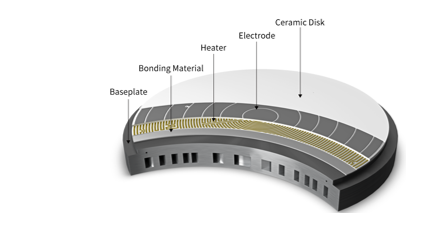
- ESC (Electrostatic Chuck) → AlN / Al₂O₃
- Heat spreaders → AlN
- Precision cooling plates → Al₂O₃ / SiC
5. Material Selection Guide (Engineering View)
- Cost-sensitive applications → Al₂O₃
- Plasma corrosion environment → Y₂O₃
- High precision structure → SiC
- Mechanical load & durability → Si₃N₄
- High thermal dissipation → AlN
6. Future Trend: Hybrid Ceramic Systems
Next-generation semiconductor equipment is shifting toward:
- Coated ceramic systems (Al₂O₃ + Y₂O₃)
- SiC structural platforms
- AlN thermal management integration
- Multi-material hybrid ceramic assemblies
This trend significantly improves equipment lifetime and process stability.
Conclusion
Advanced ceramics have become the backbone of semiconductor manufacturing equipment. Each material plays a specialized role—from structural support to plasma resistance and thermal management.
Selecting the right ceramic material directly impacts:
- Equipment lifetime
- Stabilité du processus
- Taux de rendement
- Maintenance cost
Request Custom Ceramic Components
We provide:
- Alumina ceramic parts (Al₂O₃)
- Silicon carbide precision components (SiC)
- Silicon nitride structural parts (Si₃N₄)
- Aluminum nitride thermal substrates (AlN)
- Yttria coating solutions (Y₂O₃)
👉 Custom sizes, machining, polishing, coating, and engineering support available.