xinkehui

How to Prepare an RFQ for Custom Ceramic Components

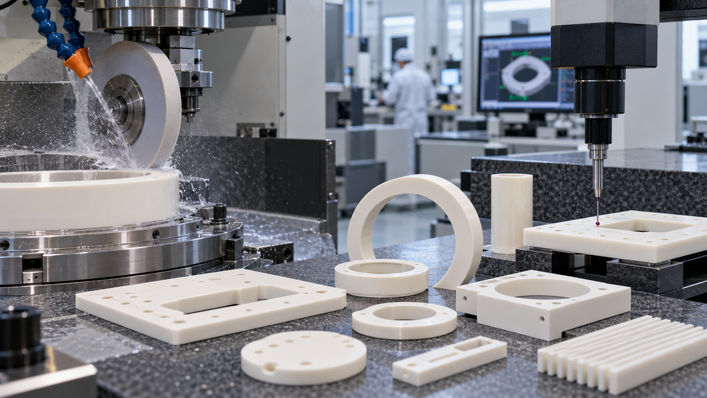
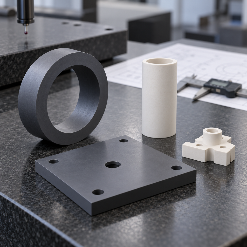
Custom ceramic components can include rings, plates, tubes, chucks, support parts and other shapes made to fit a specific machine or process. A clear request for quotation helps suppliers assess manufacturability, identify missing information and quote the correct inspection scope. Start with the part drawing. A 2D drawing should show all critical dimensions, tolerances, hole […]

How to Prepare an RFQ for Custom Ceramic Components Lire la suite »
SiC Wafer Boats and Cantilever Paddles: Key Design Points for Furnace Applications

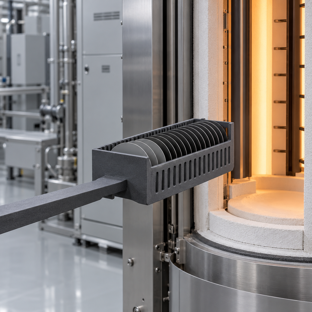
Wafer boats and cantilever paddles support wafers during loading, unloading and thermal processing. Their geometry must fit the furnace and wafer format, while the material must suit the process atmosphere and operating cycle. The first design step is confirming the equipment interface. Share the furnace type, usable hot-zone dimensions, loading direction and support arrangement. For

SiC Wafer Boats and Cantilever Paddles: Key Design Points for Furnace Applications Lire la suite »

Ceramic Wafer End Effectors: What to Specify for Reliable Wafer Handling

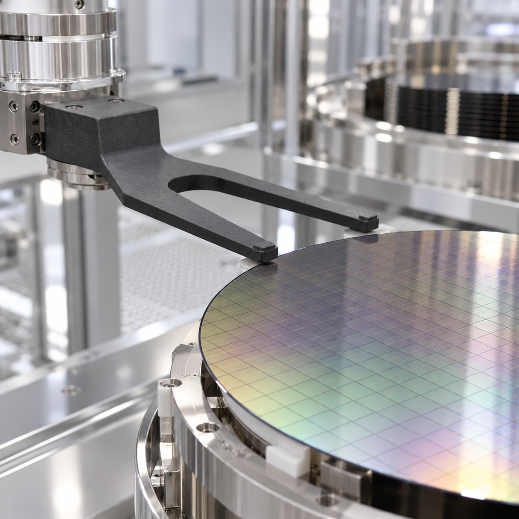
A ceramic wafer end effector supports and transfers wafers between process stations, carriers and equipment modules. Its shape may look simple, but small differences in geometry, surface condition or mounting can affect wafer positioning and transfer reliability. When selecting or specifying an end effector, start with the wafer and robot interface. Provide the wafer diameter,

Ceramic Wafer End Effectors: What to Specify for Reliable Wafer Handling Lire la suite »

Precision Ceramic Wafer Chuck and Clamp for Semiconductor Equipment

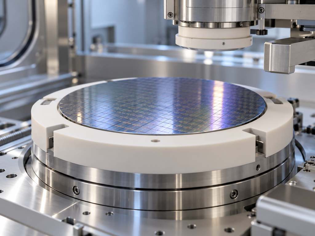
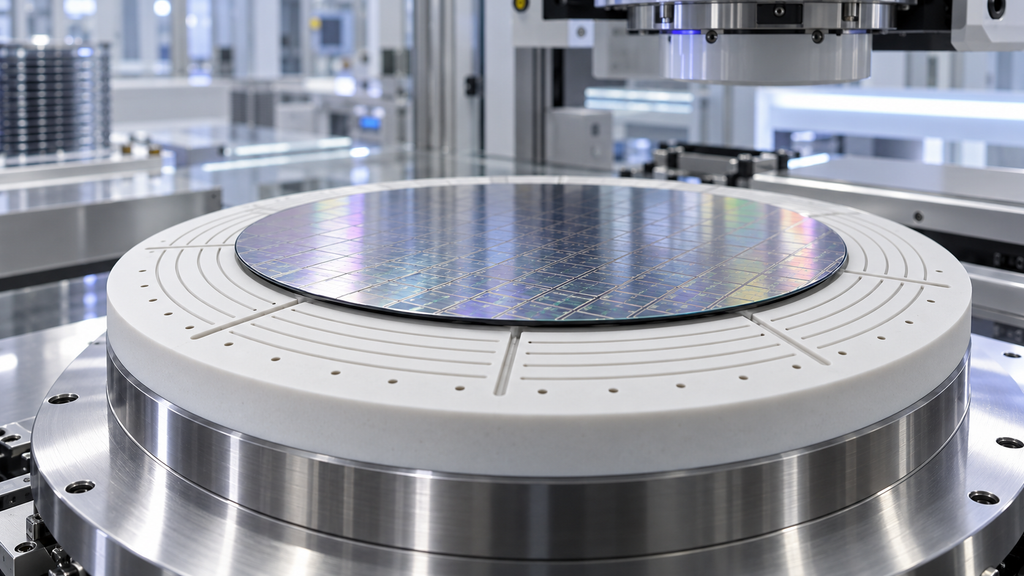
Precision ceramic wafer chucks and wafer clamps are widely used in semiconductor equipment to support, position and hold wafers during processing, inspection and handling. As wafer sizes increase and semiconductor manufacturing tolerances become tighter, the dimensional stability and surface quality of these components become increasingly important. Advanced ceramics are particularly suitable for wafer handling applications

Precision Ceramic Wafer Chuck and Clamp for Semiconductor Equipment Lire la suite »

AlN Electrostatic Chuck for Semiconductor Equipment

Aluminum nitride electrostatic chucks, commonly referred to as AlN electrostatic chucks or AlN ESCs, are widely used in advanced semiconductor processing equipment. They combine electrical insulation with high thermal conductivity, making them particularly suitable for processes where wafer temperature control is critical. Typical applications include plasma etching, CVD, PVD and other vacuum semiconductor processes. Why

AlN Electrostatic Chuck for Semiconductor Equipment Lire la suite »

300mm Electrostatic Chuck for Semiconductor Wafer Processing

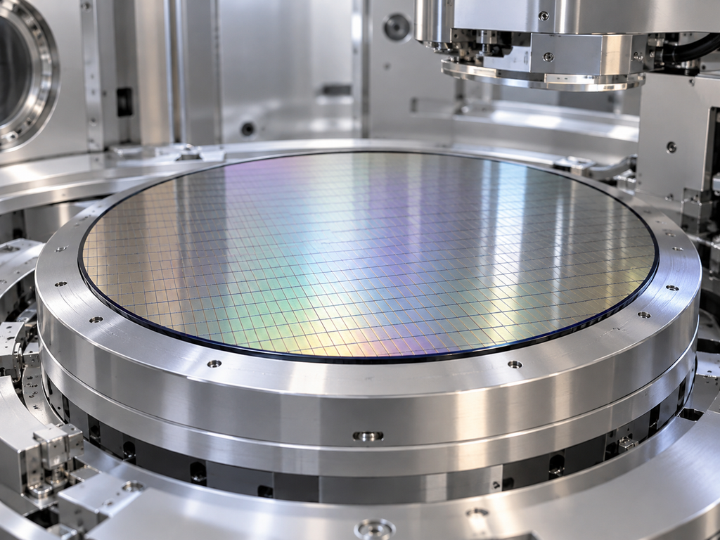
As 300mm wafers have become standard in advanced semiconductor manufacturing, wafer handling and process stability have become increasingly important. The electrostatic chuck, commonly known as an ESC, is one of the key components used to hold wafers securely during plasma etching, deposition, implantation, inspection and other semiconductor processes. A 300mm electrostatic chuck uses electrostatic force

300mm Electrostatic Chuck for Semiconductor Wafer Processing Lire la suite »

Machining Advanced Ceramics for Semiconductor Equipment: Tolerance, Surface Roughness, Edge Chipping and Dimensional Inspection

Advanced ceramics are widely used in semiconductor manufacturing equipment because of their high hardness, electrical insulation, chemical stability, wear resistance and excellent dimensional stabilit Common ceramic materials used in semiconductor equipment include: These materials are used to manufacture components such as ceramic rings, plates, vacuum chucks, insulating parts, wafer-handling components, chamber parts, nozzles, pins and

Machining Advanced Ceramics for Semiconductor Equipment: Tolerance, Surface Roughness, Edge Chipping and Dimensional Inspection Lire la suite »

Precision Ceramic Rings for Semiconductor Equipment: Alumina, AlN and SiC Material Selection for Plasma and Vacuum Applications

Precision ceramic rings are widely used in semiconductor manufacturing equipment where conventional metal components may struggle with plasma exposure, electrical insulation, high temperature, corrosion, particle control or dimensional stability. Depending on the equipment design, ceramic rings may function as focus rings, edge rings, chamber rings, insulating rings, support rings, sealing interfaces or structural components inside

Precision Ceramic Rings for Semiconductor Equipment: Alumina, AlN and SiC Material Selection for Plasma and Vacuum Applications Lire la suite »

Ceramic Vacuum Chucks for Semiconductor Wafer Handling: Flatness, Porosity, Vacuum Groove Design and Surface Finish

As semiconductor wafers become larger, thinner and more sensitive to mechanical stress, reliable wafer holding becomes increasingly important during inspection, grinding, dicing, metrology and other precision manufacturing processes. A ceramic vacuum chuck provides a stable reference surface while using negative pressure to hold the wafer securely in position. Compared with conventional metal fixtures, technical ceramics

Ceramic Vacuum Chucks for Semiconductor Wafer Handling: Flatness, Porosity, Vacuum Groove Design and Surface Finish Lire la suite »

Why 99.9% Alumina Is Not Enough: Microstructure Is Becoming the Real Specification for Semiconductor Ceramics

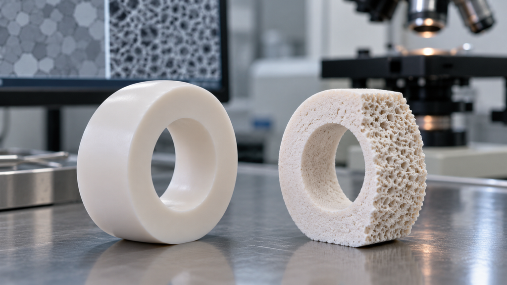
“99.9% alumina” is a common ceramic specification. For semiconductor equipment, however, this number does not tell the whole story. Two ceramic components can both contain 99.9% Al₂O₃ and still behave very differently inside a plasma-processing chamber. The reason is microstructure. Porosity, grain size, grain-boundary chemistry and sintering history can influence erosion, contamination and particle generation

Why 99.9% Alumina Is Not Enough: Microstructure Is Becoming the Real Specification for Semiconductor Ceramics Lire la suite »

YOF Ceramic Coatings for Semiconductor Etch Chambers: Why Fluorine-Containing Surfaces Are Gaining Attention

Advanced semiconductor etching requires increasingly aggressive plasma environments. Fluorine-containing gases are widely used to etch materials such as silicon oxide, silicon nitride and other semiconductor films. The same plasma that removes material from the wafer also attacks the chamber. This creates a major materials challenge. Chamber-facing components must survive chemical attack and energetic ion bombardment

YOF Ceramic Coatings for Semiconductor Etch Chambers: Why Fluorine-Containing Surfaces Are Gaining Attention Lire la suite »

Silicon Nitride Ceramic Bearings Reach 30,000 rpm: Why EV eAxles Are Becoming a Major Si₃N₄ Application

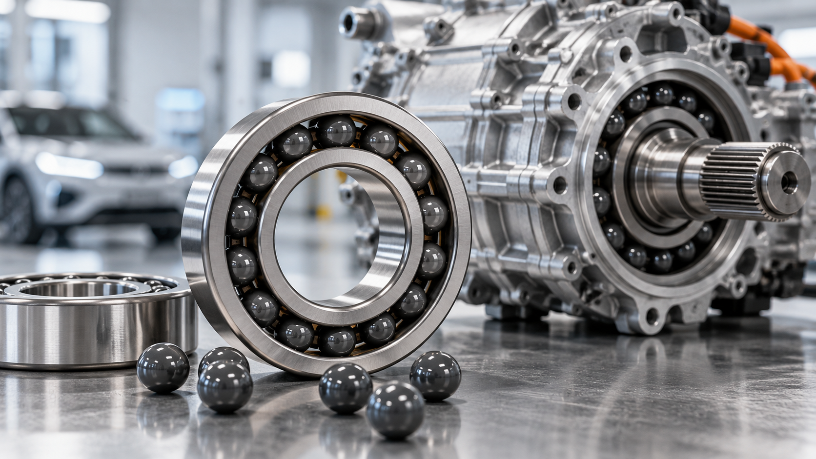
Electric-vehicle powertrains are changing the requirements placed on bearings. A conventional vehicle transmission is largely mechanical. An electric eAxle integrates: As manufacturers increase motor speed to reduce motor size and weight, bearing rotational speeds are rising sharply. In June 2026, JTEKT announced a grease-lubricated ceramic-ball bearing designed for high-performance EV eAxles with operation up to

Silicon Nitride Ceramic Bearings Reach 30,000 rpm: Why EV eAxles Are Becoming a Major Si₃N₄ Application Lire la suite »