
on implantation equipment uses accelerated ion beams to introduce controlled dopants into semiconductor wafers. Producing and transporting these beams requires high voltages, stable vacuum conditions and precise control of electrically isolated components.
Within the ion source, extraction system, acceleration column and beamline, ceramic insulators separate energized electrodes from grounded structures. These components may appear simple, but their reliability directly affects beam stability, particle control, equipment uptime and operator safety.
High-purity alumina is widely used for such insulators because it combines electrical insulation, mechanical strength, vacuum compatibility and dimensional stability. However, selecting an alumina grade based only on a published dielectric-strength value is not sufficient.
In real ion implantation systems, failures often begin at contaminated surfaces, metal–ceramic–vacuum junctions, machining defects or thermally stressed interfaces rather than through the bulk ceramic itself. Successful insulator design therefore requires coordinated control of material purity, geometry, surface finish, electric-field distribution, cleaning, mounting and operating conditions.
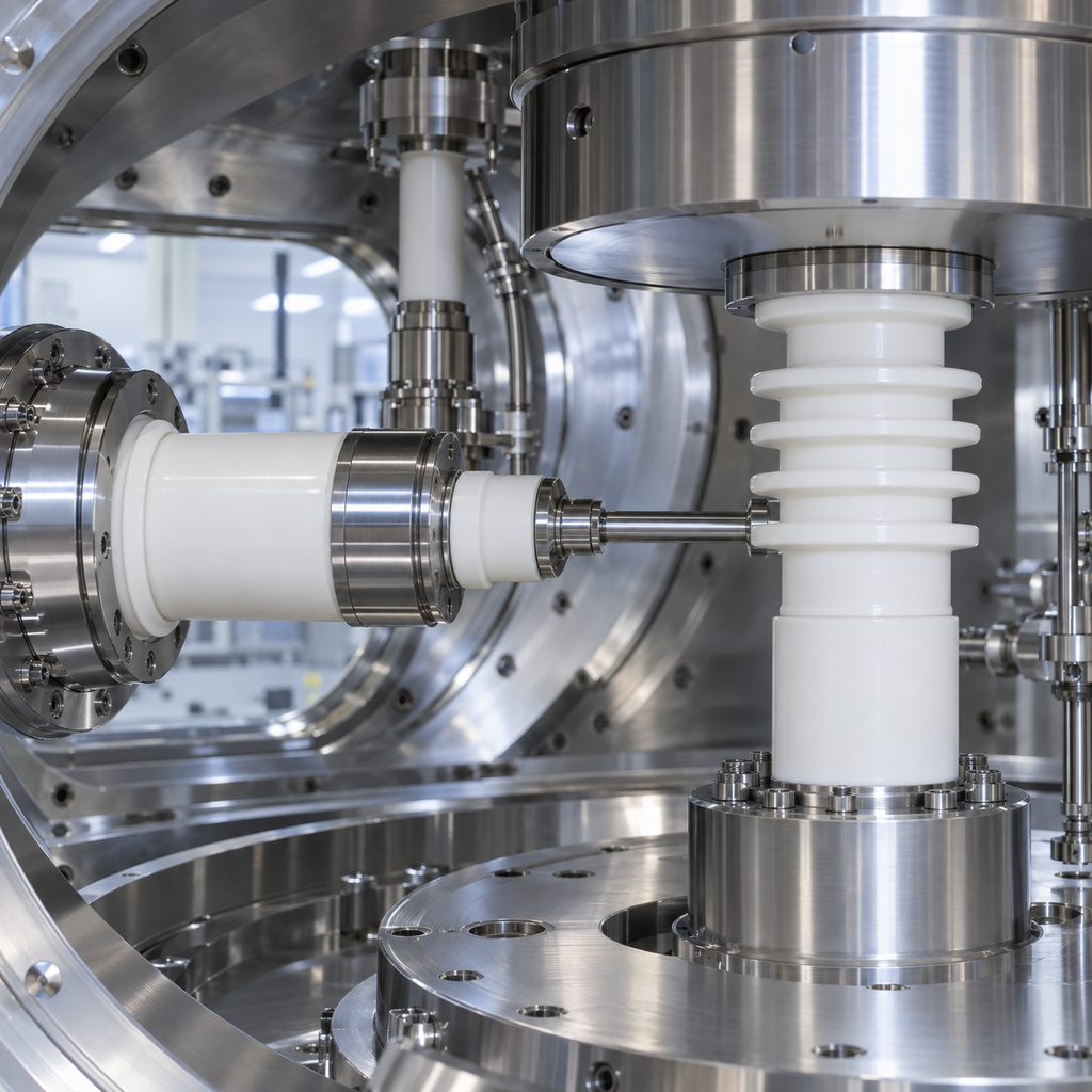
Where Ceramic Insulators Are Used in Ion Implantation Equipment
Depending on the implanter architecture, alumina components may be used in:
- Ion-source electrical isolation
- Extraction-electrode supports
- Acceleration-column insulators
- High-voltage feedthroughs
- Suppression-electrode supports
- Einzel lens and focusing assemblies
- Beam-steering components
- Faraday cup assemblies
- Vacuum gauge insulation
- High-voltage terminal supports
- Electrical connector housings
- Sensor isolation components
- Vacuum chamber interfaces
The electrical conditions vary significantly among these locations. An insulator near the ion source may experience heat, plasma, sputtered material and reactive species. An acceleration-column insulator may face a much larger voltage difference but less direct thermal loading.
The component specification must therefore be based on its actual position and function rather than on a general description such as “high-voltage ceramic insulator.”
Why Alumina Is Commonly Selected
Strong Electrical Insulation
Dense alumina has high electrical resistivity and good dielectric performance. It can electrically isolate electrodes while supporting mechanical loads in vacuum.
Electrical properties depend on:
- Alumina purity
- Density and porosity
- Grain structure
- Sintering additives
- Glassy grain-boundary phases
- Temperature
- Frequency
- Surface cleanliness
- Humidity before pump-down
- Radiation and plasma exposure
A room-temperature datasheet value cannot fully describe performance inside an operating ion implantation system.
Vacuum Compatibility
Properly densified and cleaned alumina can provide low outgassing and is suitable for high-vacuum environments. It contains no organic insulation layer that can easily soften or decompose under heat.
The complete component may nevertheless include metallization, brazes, adhesives or trapped cavities. These features can dominate the assembly’s vacuum behavior even when the alumina itself is clean and dense.
Mechanical Strength and Rigidity
Alumina provides the stiffness required to maintain electrode position and alignment. This is particularly important in acceleration and focusing assemblies, where small dimensional changes can influence electric-field distribution or beam transport.
However, alumina is brittle. It tolerates compressive loading well but is sensitive to:
- Tensile stress
- Edge damage
- Point loading
- Mounting misalignment
- Impact
- Rapid temperature changes
- Machining-induced microcracks
Mechanical mounting must allow the ceramic to support the assembly without being forced to absorb excessive distortion.
Thermal and Chemical Stability
High-purity alumina maintains useful electrical and mechanical properties over a broad temperature range. It also resists many process chemicals and cleaning agents.
Compatibility still needs to be evaluated for actual exposure conditions, especially where the ceramic is exposed to plasma, energetic ions, sputtered metals, halogens or repeated wet cleaning.
Selecting the Alumina Purity
High-voltage vacuum insulators are commonly manufactured from dense technical alumina grades. The appropriate purity may range from approximately 95% to above 99.7%, depending on voltage, vacuum level, contamination requirements and cost.
Higher-purity alumina generally provides:
- Lower levels of alkali and glass-forming impurities
- Better high-temperature electrical resistivity
- Reduced contamination risk
- Improved plasma compatibility
- Lower dielectric loss
- Greater stability under demanding vacuum conditions
Lower-purity grades may be easier and less expensive to manufacture, but their larger glassy-phase content can influence surface conductivity and high-temperature insulation.
For semiconductor equipment, purity should not be evaluated by the alumina percentage alone. The specification may also need limits for:
- Sodium
- Potassium
- Calcium
- Magnesium
- Iron
- Titanium
- Silicon
- Open porosity
- Bulk density
- Exposed inclusions
- Surface metallic contamination
A nominally high-purity material can still be unsuitable if its trace-metal profile conflicts with the process contamination budget.
Dielectric Strength: Important but Frequently Misinterpreted
Dielectric strength describes the electric field at which an insulating material experiences breakdown under defined test conditions. It is commonly reported in kV/mm.
This value is useful for comparing materials, but it should not be used as a simple design formula. Multiplying the published dielectric strength by the ceramic thickness does not automatically determine a safe operating voltage.
Measured dielectric strength depends on:
- Specimen thickness
- Electrode shape
- Electrode spacing
- Voltage waveform
- Voltage ramp rate
- AC, DC or pulsed operation
- Test frequency
- Temperature
- Atmosphere
- Surface finish
- Material defects
- Test duration
Small laboratory specimens tested under controlled conditions may achieve substantially different results from a large, machined insulator operating under vacuum.
Bulk Breakdown Versus Surface Flashover
Bulk breakdown occurs when an electrical path develops through the ceramic body. Possible contributors include pores, inclusions, cracks, insufficient thickness and local field concentration.
Surface flashover occurs along the ceramic surface. In high-voltage vacuum equipment, it can happen at an applied voltage much lower than the theoretical bulk breakdown voltage.
Surface flashover is often the more relevant design limitation because the ceramic surface may collect:
- Sputtered metal
- Carbon-rich deposits
- Process residue
- Condensed precursor material
- Cleaning residue
- Moisture before evacuation
- Handling contamination
- Microscopic particles
These deposits can create partially conductive paths that reduce effective creepage resistance.
High Voltage Behaves Differently in Vacuum
It is tempting to assume that vacuum always improves insulation because there is less gas available for an electrical discharge. Actual behavior is more complicated.
At reduced pressure, discharge behavior depends on pressure, gap length, electrode geometry and gas composition. Under high vacuum, breakdown may be driven by mechanisms such as:
- Field emission from sharp metal features
- Electron multiplication near surfaces
- Secondary electron emission
- Desorption of gas from the ceramic
- Localized vapor from electrode microprotrusions
- Charged-particle accumulation
- Triple-junction field enhancement
- Conductive surface deposits
For this reason, an insulator that performs adequately in air may not provide the same reliability in a high-voltage vacuum assembly.
Qualification should reproduce the expected pressure range, electrode design, polarity, ramp rate, surface condition and operating temperature.
The Triple-Junction Problem
A critical location in many vacuum insulators is the junction where three regions meet:
- Metal electrode
- Ceramic insulator
- Vacuum
This metal–ceramic–vacuum intersection is commonly called a triple junction.
Electric fields can become concentrated at this location. Electrons emitted near the metal edge may strike the ceramic surface, release secondary electrons and contribute to a surface-flashover sequence.
Triple-junction risk can be reduced through:
- Rounded metal-electrode edges
- Recessed ceramic interfaces
- Guard rings
- Shielding electrodes
- Controlled field grading
- Longer surface paths
- Elimination of sharp metallization boundaries
- Accurate concentricity
- Smooth ceramic surfaces
- Clean assembly procedures
Insulator geometry and electrode geometry should therefore be developed together. Increasing ceramic thickness alone may not solve a field-concentration problem.
Surface Tracking and Creepage Distance
Surface tracking is the gradual formation of a conductive path along an insulating surface. In atmosphere, it is often associated with moisture and contamination. In ion implantation equipment, deposited conductive material and energetic particle exposure can create similar reliability problems.
Why Grooves Are Added
High-voltage ceramic insulators often use ribs, corrugations or grooves. These features can:
- Increase creepage distance
- Interrupt direct deposition paths
- Reduce line-of-sight coating
- Shield portions of the ceramic surface
- Change the electric-field distribution
Grooves must be designed carefully. Narrow, deep features may be difficult to machine and clean. Sharp groove roots can concentrate mechanical stress and encourage crack initiation.
A suitable groove design considers:
- Minimum root radius
- Rib thickness
- Machining-tool access
- Cleaning access
- Expected deposition direction
- Electric-field simulation
- Thermal gradients
- Inspection requirements
Line-of-Sight Deposition
In ion-source and beamline environments, sputtered or evaporated material may coat exposed surfaces. A thin conductive film across the wrong area can greatly reduce high-voltage reliability.
Design measures may include:
- Recessing the active insulating surface
- Adding replaceable shields
- Using staggered ribs
- Avoiding a direct path between electrodes
- Increasing the protected creepage distance
- Providing access for periodic cleaning
- Monitoring leakage current over time
The longest geometric path is not always the most effective path. A shorter protected surface may outperform a longer surface directly exposed to deposition.
Vacuum Outgassing
Stable vacuum is essential for beam formation, ion transport and process repeatability. Gas released from an insulator or its assembly can increase pump-down time and contribute to unstable high-voltage behavior.
Potential gas sources include:
- Adsorbed water
- Machining coolant residue
- Cleaning chemicals
- Fingerprints and handling contamination
- Organic packaging material
- Porous metallization
- Brazing residue
- Trapped gas in blind holes
- Adhesives
- Microcracks and interconnected pores
Dense alumina has good intrinsic vacuum compatibility, but the manufacturing and cleaning history determines the condition of the delivered component.
Designing Against Virtual Leaks
A virtual leak is gas trapped in a volume that communicates only slowly with the main vacuum chamber. It can imitate a true leak and prolong pump-down.
Potential problem features include:
- Blind threaded holes
- Unvented mounting interfaces
- Overlapping ceramic and metal surfaces
- Closed internal cavities
- Trapped volumes behind seals
- Poorly vented fasteners
Where possible, designs should include vent paths and avoid unnecessary closed spaces.
Vacuum Qualification Methods
Depending on application severity, qualification may include:
- Controlled bake-out
- Pump-down testing
- Helium leak testing
- Residual gas analysis
- Mass-loss evaluation
- Outgassing-rate measurement
- Inspection after thermal cycling
Testing should be performed on the finished assembly when brazes, metallized areas or seals are involved. Testing an unassembled ceramic sample cannot reveal emissions from joining materials or trapped volumes.
Surface Finish and Machining Quality
The surface condition affects dielectric performance, contamination retention and mechanical strength.
Potential machining defects include:
- Edge chips
- Grinding cracks
- Deep scratches
- Pits
- Tool marks
- Sharp internal corners
- Subsurface damage
- Contaminated abrasive residue
A very rough surface can trap contamination and increase local field irregularity. However, specifying a mirror polish on every surface may add cost without improving performance.
Surface requirements should distinguish among:
- High-field insulating surfaces
- Metal-bonding surfaces
- Mounting surfaces
- Vacuum-exposed surfaces
- Noncritical exterior surfaces
Critical high-voltage surfaces may require defined roughness, visual inspection criteria and restrictions on scratches or chips. All edges should have controlled radii or chamfers appropriate to the mechanical and electrical design.
Thermal Shock in Ion Implantation Equipment
Ceramic insulators may experience temperature changes caused by:
- Ion-source heating
- Beam interception
- Electrode heating
- Plasma exposure
- Radiant heat
- Chamber bake-out
- Cooling-system operation
- Rapid equipment shutdown
- Cleaning and maintenance cycles
Alumina is thermally stable, but its resistance to rapid temperature change is limited by its thermal conductivity, thermal expansion, elastic modulus, strength and component geometry.
Common Thermal-Stress Locations
Cracks frequently begin near:
- Sharp corners
- Thin-to-thick section transitions
- Deep groove roots
- Mounting holes
- Brazed joints
- Metal inserts
- Areas directly exposed to heat
- Regions constrained by rigid hardware
Large ceramic parts may develop substantial internal temperature gradients even when the average temperature remains within the material’s operating limit.
Improving Thermal-Shock Reliability
Useful design measures include:
- Generous transition radii
- Uniform wall thickness where practical
- Gradual heating and cooling
- Reduced direct beam interception
- Thermal shielding
- Flexible mounting
- CTE-compatible joining materials
- Controlled brazing geometry
- Avoidance of point contact
- Thermal modeling of local hot spots
The qualification plan should specify the actual ramp rate and temperature difference rather than only the maximum operating temperature.
Metalized and Brazed Alumina Insulators
Some high-voltage assemblies require hermetic metal-to-ceramic joints. Alumina may be metallized and brazed to stainless steel, Kovar, molybdenum or another compatible metal system.
Important variables include:
- Metallization composition
- Metallization adhesion
- Braze-alloy selection
- Joint clearance
- Wetting behavior
- Ceramic surface preparation
- Metal-wall thickness
- CTE mismatch
- Residual stress
- Vacuum cleanliness
- High-voltage field distribution
A mechanically strong braze is not necessarily an electrically optimized braze. Excess brazing alloy, sharp fillets or exposed metallization can create high-field features.
Testing may need to include:
- Joint-strength evaluation
- Hermetic leak testing
- Thermal cycling
- High-voltage withstand
- Insulation resistance
- Cross-sectional analysis
- Visual inspection for braze overflow
- Dimensional inspection after joining
Mechanical Mounting
Because alumina is brittle, metal hardware should not force it into alignment.
Recommended design principles include:
- Use broad, controlled contact surfaces
- Avoid direct point loading
- Apply defined fastener torque
- Use compliant washers or interfaces where appropriate
- Allow differential thermal expansion
- Maintain electrode concentricity
- Prevent impact during installation
- Avoid metal burrs contacting the ceramic
- Do not clamp across visibly damaged edges
The drawing should define functional datums, perpendicularity, concentricity and interface flatness. Otherwise, dimensional variation can move the ceramic into a region of higher electrical or mechanical stress.
Common Failure Modes
Surface Flashover
Possible causes include conductive deposits, inadequate creepage distance, triple-junction field concentration, surface damage or poor cleaning.
Bulk Dielectric Breakdown
Possible causes include insufficient wall thickness, internal defects, excessive electric field, cracks or inappropriate material grade.
Vacuum Instability
Possible causes include adsorbed moisture, trapped volumes, porous joints, organic contamination or inadequate bake-out.
Ceramic Cracking
Possible causes include mounting stress, rapid temperature change, impact, machining damage or metal–ceramic CTE mismatch.
Leakage-Current Increase
Possible causes include surface deposition, moisture, thermal damage, radiation exposure or gradual formation of a conductive path.
Particle Generation
Possible causes include chipped ceramic edges, rubbing at mounting interfaces, surface erosion or repeated thermal cracking.
Failure analysis should examine the ceramic, electrode, surface deposits, vacuum history and operating-voltage record as one system.
Recommended Qualification Plan
Material Verification
- Alumina purity
- Bulk density
- Open porosity
- Trace-element composition
- Material lot identification
- Microstructure where required
Dimensional Inspection
- Overall diameter and length
- Wall thickness
- Flatness
- Perpendicularity
- Concentricity
- Groove dimensions
- Mounting-hole locations
- Critical radii and chamfers
Surface Inspection
- Surface roughness
- Chips and cracks
- Scratches and pits
- Grinding damage
- Cleanliness
- Metallization condition
Electrical Testing
- Volume resistivity
- Surface resistance
- Dielectric strength
- Insulation resistance
- High-voltage withstand
- Leakage current
- Partial-discharge behavior where applicable
Electrical test conditions should define temperature, atmosphere, pressure, polarity, ramp rate, dwell time and acceptance criteria.
Vacuum Testing
- Helium leak rate for sealed assemblies
- Pump-down behavior
- Outgassing evaluation
- Residual gas analysis when required
- Testing before and after bake-out
- Retesting after thermal cycling
Thermal and Mechanical Testing
- Maximum-temperature dwell
- Heating and cooling cycles
- Specified thermal ramp rate
- Mechanical proof load
- Joint-strength verification
- Inspection after cycling
- High-voltage retest after cycling
System-Level Validation
The most meaningful final test uses the intended electrode arrangement and representative vacuum conditions. It should monitor:
- Stable operating voltage
- Leakage current
- Arc or flashover events
- Vacuum pressure
- Temperature
- Particle generation
- Performance after controlled contamination or service cycles
Information to Include in an RFQ
For an accurate quotation and manufacturability review, provide:
- Ion implantation equipment location
- Function of the insulator
- Normal and maximum operating voltage
- AC, DC or pulsed waveform
- Voltage polarity
- Required current isolation
- Operating pressure range
- Process-gas composition
- Normal and maximum temperature
- Heating and cooling rates
- Expected plasma or ion exposure
- Sputtered-material exposure
- Required alumina purity
- Trace-metal limits
- Minimum creepage distance
- Surface-finish requirements
- Dimensional tolerances
- Metallization and brazing requirements
- Helium leak-rate limit
- Outgassing or bake-out requirements
- Cleaning and packaging standard
- Expected service life
- Thermal-cycle test conditions
- High-voltage acceptance-test conditions
- 2D drawings and 3D models
- Prototype and annual quantity
The RFQ should distinguish mandatory acceptance criteria from preferred engineering targets.
Frequently Asked Questions
Is 99.5% alumina sufficient for a high-voltage ion implanter insulator?
It may be sufficient for some positions, but purity alone cannot determine suitability. Voltage, temperature, vacuum level, contamination limits, geometry and surface exposure must also be considered. More demanding ion-source or high-temperature locations may justify a higher-purity grade.
Can the datasheet dielectric strength be used to calculate the required wall thickness?
Not directly. Published values normally come from controlled test specimens. A finished component may be limited by surface flashover, triple-junction fields, defects or contamination before bulk breakdown occurs.
Why does an insulator flash over even though the ceramic is not cracked?
A conductive surface deposit, moisture, field-emission site or poorly designed electrode edge may initiate discharge along the surface. The ceramic body can remain structurally intact while its surface-insulation performance has deteriorated.
Do deeper grooves always improve high-voltage performance?
No. Grooves may increase creepage distance and shield surfaces, but overly deep or sharp grooves can be difficult to clean and may create thermal or mechanical stress concentrations. Geometry should be verified through electric-field analysis and practical testing.
Does high-purity alumina have zero outgassing?
No material surface is completely free of adsorbed gases. Dense high-purity alumina can provide very low outgassing after proper cleaning and bake-out, but residues, metallization, joints and trapped volumes must also be controlled.
Should electrical testing be performed in air or vacuum?
Incoming testing in air may be useful, but it does not replace qualification under the intended vacuum pressure and electrode configuration. Vacuum surface-flashover mechanisms can differ substantially from atmospheric breakdown.
Can used alumina insulators be cleaned and reused?
Possibly, depending on the deposited material and the approved cleaning process. After cleaning, the part should be inspected for surface damage, dimensional change, cracks, residual contamination and deterioration of metallized or brazed areas. Critical components may also require renewed high-voltage and vacuum testing.
Conclusion
High-voltage alumina ceramic insulators are essential to the electrical stability of ion implantation equipment. Their performance depends on much more than nominal alumina purity or a single dielectric-strength value.
Reliable operation requires coordinated control of:
- Alumina composition and density
- Bulk and surface electrical properties
- Creepage-path geometry
- Triple-junction electric fields
- Vacuum outgassing
- Surface contamination
- Machining quality
- Metalized and brazed interfaces
- Mechanical mounting
- Thermal gradients
- Cleaning and maintenance procedures
For equipment manufacturers and replacement-part buyers, the best procurement approach is to define measurable operating and acceptance conditions. High-voltage performance should be verified using the real pressure range, temperature, electrode geometry and surface environment whenever possible.
A properly engineered alumina insulator can provide stable electrical isolation, reduced vacuum contamination and long service life. A component selected only from a generic material datasheet may fail even when its nominal material properties appear adequate.

