
Polished alumina substrates are widely used in semiconductor equipment, power electronics, thin-film circuits, sensors, optoelectronics and precision industrial components. They provide electrical insulation, mechanical strength, dimensional stability and resistance to heat and chemicals.
However, “polished alumina substrate” is not a complete purchasing specification. Two substrates with the same length, width and thickness may behave very differently because of variations in purity, density, flatness, surface roughness, edge finishing and polishing quality.
These parameters influence thin-film adhesion, photolithography accuracy, metallization uniformity, component bonding and final device reliability. Buyers should therefore define both dimensional and surface requirements before requesting a quotation.
This guide explains the most important specifications for custom polished Al₂O₃ substrates.
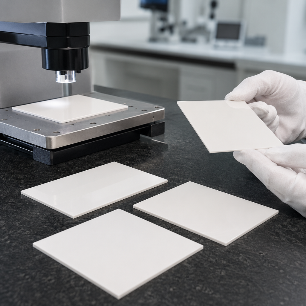
What Is a Polished Alumina Substrate?
A polished alumina substrate is a flat ceramic plate manufactured from aluminum oxide and finished using precision grinding, lapping or polishing.
Depending on the application, the substrate may be:
- As-fired
- Surface-ground
- Lapped
- Single-side polished
- Double-side polished
- Laser-cut
- Mechanically machined
- Metallized after polishing
The correct surface condition depends on the downstream process. A substrate used as a mechanical insulating plate does not need the same surface quality as one used for thin-film deposition or semiconductor inspection equipment.
Polishing can improve:
- Surface smoothness
- Thickness consistency
- Flatness
- Parallelism
- Cleanliness
- Thin-film uniformity
- Bonding performance
- Optical inspection accuracy
Polishing does not automatically guarantee that every surface or dimensional parameter meets a demanding specification. Each requirement should be stated separately.
1. Alumina Purity
Alumina substrates are available in several purity levels. Common compositions include 96%, 99%, 99.5%, 99.6% and 99.8% or higher alumina.
The remaining material consists mainly of sintering additives and secondary phases used to support densification and manufacturing.
96% Alumina
A 96% alumina substrate provides a practical balance of cost, mechanical performance and electrical insulation.
It is commonly used for:
- Thick-film circuits
- Electrical insulation
- General electronic components
- Industrial sensors
- Heater substrates
- Standard power electronics
It is generally more economical and easier to manufacture than higher-purity grades. However, its secondary phases may reduce thermal conductivity, chemical resistance and surface consistency.
99% to 99.6% Alumina
Higher-purity alumina is often selected for applications requiring improved dielectric performance, chemical resistance and surface quality.
Typical applications include:
- Semiconductor equipment components
- Thin-film circuits
- Vacuum-compatible parts
- High-voltage insulation
- Precision sensor substrates
- Optical and laser components
These grades generally contain fewer glassy phases than 96% alumina and can provide a more stable polished surface.
99.8% and Higher-Purity Alumina
Very-high-purity alumina may be required when contamination control, plasma resistance or demanding thin-film processing is involved.
Potential applications include:
- Semiconductor process equipment
- High-vacuum systems
- Analytical instruments
- High-temperature electronics
- Specialized thin-film devices
Higher purity does not automatically make a substrate suitable for every application. Grain size, density, porosity and surface preparation remain important.
2. Density and Porosity
Density affects mechanical strength, dielectric behavior, surface quality and chemical resistance. A dense substrate normally produces a more consistent polished surface.
Open pores can create several problems:
- Trapping cleaning chemicals
- Retaining particles
- Producing pits during polishing
- Creating discontinuities in deposited films
- Reducing vacuum compatibility
- Increasing local electric-field concentration
When surface quality is important, buyers should consider specifying:
- Bulk density
- Apparent porosity
- Water absorption
- Maximum allowable surface pits
- Maximum pore size
- Inspection method
A very low average surface roughness cannot by itself guarantee the absence of isolated pores or pits. Both roughness and local defect limits may be necessary.
3. Substrate Dimensions
A complete dimensional specification should include:
- Length and width
- Thickness
- Length and width tolerances
- Thickness tolerance
- Corner radius
- Chamfer or bevel dimensions
- Hole dimensions, if required
- Slot or notch position
- Reference datum
- Measurement temperature
Ceramics are harder and more brittle than many metals and plastics. Unnecessarily tight tolerances can significantly increase manufacturing cost.
The drawing should distinguish between functionally critical dimensions and general dimensions.
4. Thickness and Thickness Tolerance
Substrate thickness influences:
- Mechanical strength
- Thermal resistance
- Electrical insulation
- Handling stability
- Flatness
- Weight
- Compatibility with downstream equipment
Thin substrates offer a shorter heat-transfer path but are more fragile and more sensitive to warpage. Thick substrates provide greater stiffness but may increase thermal resistance.
Thickness should be measured at multiple locations rather than at only one point. The buyer should also clarify whether the requirement refers to:
- Nominal thickness
- Average thickness
- Local thickness
- Total thickness variation
- Thickness after final polishing
For double-side-polished substrates, thickness control is closely related to parallelism and TTV.
5. Total Thickness Variation
Total thickness variation, or TTV, is the difference between the maximum and minimum measured thickness across the substrate.
TTV is important for:
- Photolithography
- Thin-film deposition
- Wafer bonding
- Vacuum chucking
- Precision mounting
- Automated handling
- Maintaining a consistent focal plane
A substrate may have an acceptable average thickness but still exhibit excessive local variation. This can create uneven contact or alignment errors in downstream equipment.
The TTV requirement should be defined together with:
- Measurement area
- Edge exclusion
- Number of measurement points
- Measurement equipment
- Whether the substrate is free-standing or supported
6. Flatness
Flatness describes how much a surface deviates from an ideal plane. It is one of the most important parameters for precision alumina substrates.
Poor flatness can cause:
- Uneven contact with fixtures
- Vacuum leakage
- Nonuniform film deposition
- Die-attach voids
- Focus errors during lithography
- Uneven pressure during bonding
- Difficulty in automated handling
Flatness is not the same as surface roughness. A substrate may have a highly polished surface while still being curved or warped across its full area.
Flatness specifications should state:
- Maximum allowable deviation
- Measurement area
- Edge exclusion
- Supported or unsupported measurement condition
- Measurement method
- Reference temperature
Larger and thinner substrates are generally more difficult to manufacture to tight flatness tolerances than small, thick substrates.
7. Bow and Warp
Bow and warp describe the overall shape of a free-standing substrate.
Bow usually refers to a generally concave or convex shape. Warp represents more complex deviation from a reference plane.
These parameters become increasingly important as the substrate becomes larger or thinner.
Excessive bow or warp can cause:
- Poor vacuum chuck contact
- Robotic handling errors
- Nonuniform metallization
- Mechanical stress during assembly
- Reduced bonding yield
- Edge lifting
- Breakage during clamping
The RFQ should state whether bow and warp are measured before or after polishing, cleaning or thermal processing.
8. Parallelism
Parallelism describes the relationship between the two major surfaces. Good parallelism is particularly important when the substrate must be held between fixtures or aligned in precision equipment.
Poor parallelism can result in:
- Uneven clamping pressure
- Assembly misalignment
- Inaccurate thickness measurement
- Localized contact stress
- Variable bond-line thickness
Double-side polishing is often used when both surface quality and parallelism are critical.
Parallelism should not be assumed from a tight thickness tolerance. It should be stated as a separate requirement when functionally important.
9. Surface Roughness
Surface roughness measures small-scale height variations on the substrate surface. Ra is one of the most commonly specified roughness parameters.
The required Ra depends strongly on the downstream application.
Ground Surface
A ground surface may be appropriate for:
- Mechanical insulation
- Structural mounting
- Noncritical bonding
- Applications without thin films
It is generally more economical but may show directional grinding marks.
Lapped Surface
Lapping improves flatness and reduces roughness compared with grinding. It can provide a controlled matte finish suitable for certain bonding and coating processes.
Polished Surface
A polished surface is often required for:
- Thin-film deposition
- Photolithography
- Precision sensors
- Optical inspection
- Fine-line metallization
- Wafer-related equipment
A lower Ra value does not always guarantee better adhesion. Some coating or bonding processes require a controlled surface texture.
Buyers should confirm the optimum roughness range with the metallization, deposition or bonding process provider.
10. Ra Is Not the Only Surface Parameter
Ra represents an average and may not reveal isolated defects. Two substrates with the same Ra can have different practical surface quality.
Additional parameters may include:
- Rq: root mean square roughness
- Rz: average maximum profile height
- Maximum peak height
- Maximum valley depth
- Waviness
- Surface pit density
- Maximum scratch dimensions
- Grain pullout limits
For demanding applications, surface quality should be evaluated using both numerical roughness data and microscopic inspection.
The RFQ should also specify:
- Scan length
- Measurement area
- Filter or cutoff settings
- Measurement direction
- Contact or noncontact method
- Number of measurement positions
Without a defined test method, roughness values from different instruments may not be directly comparable.
11. Single-Side vs. Double-Side Polishing
Single-Side Polishing
Single-side polishing is suitable when only one surface is used for deposition, bonding or precision contact.
Its advantages include:
- Lower manufacturing cost
- Shorter processing time
- One functional polished surface
- A rougher backside that may assist certain mounting methods
The RFQ should clearly identify which surface is polished.
Double-Side Polishing
Double-side polishing is used when both major surfaces require controlled smoothness, thickness uniformity or parallelism.
It is appropriate for:
- Double-sided metallization
- Precision spacer components
- Optical or analytical systems
- High-accuracy assembly
- Applications requiring low TTV
Double-side polishing generally costs more because both surfaces and the final thickness must be controlled simultaneously.
12. Surface Defects
Polished alumina may contain defects originating from material preparation, sintering, machining or polishing.
Common defects include:
- Scratches
- Pits
- Pores
- Chips
- Stains
- Embedded particles
- Polishing marks
- Grain pullout
- Microcracks
- Edge fractures
A simple “scratch-free” requirement is difficult to inspect objectively. Buyers should define measurable acceptance criteria where surface defects affect performance.
Possible criteria include:
- Maximum scratch width and length
- Maximum pit diameter
- Maximum number of pits per surface
- Inspection magnification
- Illumination conditions
- Critical inspection area
- Edge exclusion
- Reference defect samples
Cosmetic standards should be separated from functional defect requirements.
13. Edge Quality
Edge condition strongly affects the handling strength and reliability of alumina substrates. Sharp, damaged or poorly finished edges can become crack-initiation points.
Important edge features include:
- Chamfer
- Bevel
- Corner radius
- Edge roughness
- Maximum chip size
- Microcrack limits
- Edge straightness
- Transition between polished faces and edges
A small controlled chamfer can improve handling safety and reduce edge chipping. However, an excessively large chamfer may reduce the usable surface area.
For substrates processed by laser cutting, the buyer should confirm whether the edge must undergo additional grinding or polishing. Laser-cut edges may show taper, recast material or localized thermal effects depending on the process.
14. Corner Design
Sharp 90-degree corners are more vulnerable to impact damage. Rounded or chamfered corners can improve handling yield.
The appropriate design depends on:
- Available mounting area
- Equipment fixture geometry
- Circuit layout
- Required edge exclusion
- Automated handling method
- Packaging configuration
Corner radius and corner chipping should be shown clearly on the drawing.
15. Cleanliness Requirements
After polishing, substrates must be cleaned to remove abrasive residue, ceramic particles, oils and handling contamination.
A controlled cleaning process may include:
- Removal of polishing residue
- Application-compatible chemical cleaning
- High-purity water rinsing
- Ultrasonic or megasonic cleaning where appropriate
- Filtered drying
- Final inspection
- Clean packaging
The cleaning method must be compatible with the alumina composition and downstream process.
For thin-film or semiconductor applications, buyers may also specify limits for:
- Particles
- Ionic contamination
- Organic residue
- Metallic contamination
- Surface stains
- Water marks
Handling with clean gloves and nonabrasive tools is necessary after final cleaning.
16. Packaging and Transportation
Polished surfaces can be scratched by contact with other substrates or unsuitable packaging materials.
Packaging should prevent:
- Substrate-to-substrate contact
- Movement during transportation
- Edge impact
- Surface abrasion
- Moisture exposure
- Particle contamination
- Static-related contamination where relevant
Possible packaging methods include:
- Individual clean bags
- Separated wafer-style carriers
- Custom plastic trays
- Nonabrasive interleaving materials
- Vacuum-sealed clean packaging
- Double-bag cleanroom packaging
Thin substrates may require rigid external support to prevent bending or breakage during shipment.
17. Inspection Methods
Different specifications require different inspection equipment.
Dimensional Inspection
Length, width, thickness, holes and feature positions may be measured with coordinate measuring equipment, optical systems or precision gauges.
Flatness Inspection
Flatness may be evaluated using:
- Optical interferometry
- Noncontact scanning systems
- Coordinate measurement
- Precision reference surfaces
- Application-specific flatness instruments
Surface Roughness Inspection
Surface roughness may be measured with:
- Contact profilometers
- Optical profilometers
- White-light interferometers
- Atomic force microscopy for specialized applications
Defect Inspection
Surface and edge defects can be inspected with:
- Controlled visual inspection
- Optical microscopy
- Automated imaging
- Edge inspection systems
- Reference defect standards
The inspection method and sampling plan should be agreed upon before production.
18. Typical Application Requirements
Thin-Film Circuits
Important parameters usually include:
- High purity
- Low surface roughness
- Low TTV
- Good flatness
- Controlled surface defects
- High cleanliness
Thick-Film Circuits
A slightly textured surface may support paste adhesion. Extremely low roughness may not be necessary.
Semiconductor Equipment
Key requirements may include:
- High purity
- Dimensional stability
- Controlled particle performance
- Chemical resistance
- Edge integrity
- Vacuum compatibility
Power Electronics
Important parameters include:
- Electrical insulation
- Thermal conductivity
- Thickness tolerance
- Flatness
- Metallization compatibility
- Thermal cycling reliability
Sensors and Optoelectronics
These applications may require:
- Precise thickness
- Low roughness
- Tight flatness
- Good parallelism
- Controlled optical inspection quality
Polished Alumina Substrate RFQ Checklist
To receive an accurate quotation, provide the following information:
- Alumina purity
- Material grade
- Length and width
- Thickness
- Dimensional tolerances
- TTV requirement
- Flatness requirement
- Bow and warp limits
- Parallelism
- Single-side or double-side polishing
- Surface roughness requirement
- Roughness measurement method
- Surface defect criteria
- Edge type
- Chamfer or bevel dimensions
- Corner radius
- Maximum edge-chip size
- Hole, slot or notch requirements
- Metallization requirements
- Cleaning standard
- Packaging method
- Inspection report requirements
- Application
- Prototype and production quantities
A technical drawing should identify the polished surface, inspection area, edge exclusion and critical dimensions.
Conclusion
Selecting a polished alumina substrate requires more than choosing its length, width and thickness. Purity, density, TTV, flatness, parallelism, roughness and edge condition can all affect downstream performance.
High-purity alumina is often preferred for semiconductor, thin-film and vacuum applications, while 96% alumina remains a practical option for cost-sensitive electronic and industrial components. Single-side polishing is suitable when only one functional surface is required, while double-side polishing provides better control of parallelism and thickness consistency.
The most effective specification defines only the parameters that influence the application and includes clear measurement methods and acceptance criteria. This approach reduces unnecessary manufacturing cost while ensuring the substrate is compatible with deposition, metallization, bonding and assembly processes.

