
In advanced semiconductor manufacturing, key process modules such as plasma etching, chemical vapor deposition (CVD), and ion implantation operate under extreme environments involving high-energy plasma, corrosive gases, high voltage bias, and rapid thermal cycling. These conditions impose stringent requirements on structural materials in terms of dielectric stability, corrosion resistance, thermal compatibility, and long-term dimensional reliability.
Advanced engineering ceramics—such as alumina (Al₂O₃), aluminum nitride (AlN), silicon carbide (SiC), and silicon nitride (Si₃N₄)—have become indispensable due to their excellent combination of thermal, electrical, and chemical stability. However, the ongoing evolution of semiconductor equipment toward miniaturization and functional integration has driven ceramic components from simple geometries to highly complex architectures, including micro-channel networks, porous arrays, thin-walled structures, and multi-curvature surfaces.
These geometric complexities, combined with the intrinsic brittleness and low fracture toughness of ceramics, have transformed manufacturing into a multi-scale engineering challenge. This paper reviews the key technical bottlenecks and enabling technologies across three core stages: forming, sintering, and precision machining.
1. Introduction: From Functional Materials to Structural Limitations
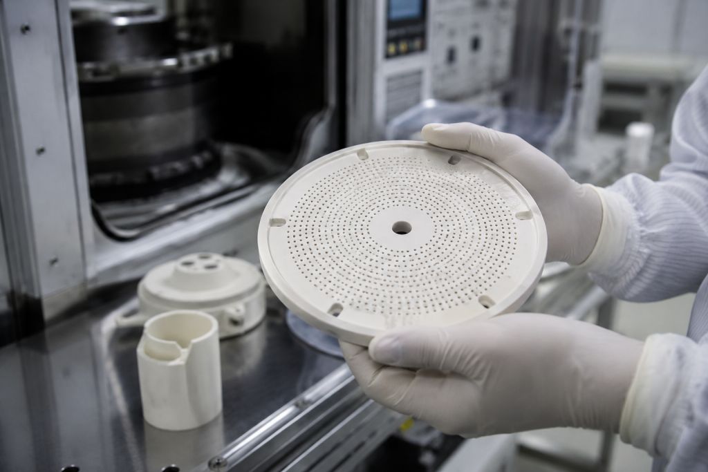
Ceramic materials are widely recognized for their exceptional hardness, high modulus, excellent wear resistance, and chemical inertness. In semiconductor equipment, they are commonly used in electrostatic chucks (ESCs), shower heads, focus rings, insulating rings, and sensor housings.
However, as device architectures become more sophisticated, ceramic components are no longer limited to simple disks, rings, or blocks. Instead, they now require:
- High-density micro-hole arrays
- Thin-walled hollow geometries
- Complex non-axisymmetric surfaces
- Embedded gas or coolant flow channels
- Multi-scale functional interfaces
This transformation significantly increases the difficulty of fabrication, as even minor density gradients or thermal mismatches during processing can lead to cracking, warping, or catastrophic failure.
2. Forming Technologies: Toward Near-Net-Shape Manufacturing of Complex Geometries
The forming stage is critical for defining the final geometry and internal homogeneity of ceramic components. Conventional processes such as dry pressing and slip casting are increasingly insufficient due to mold limitations and non-uniform green body density distribution.
2.1 Gel Casting (Gel Injection Molding)
Gel casting is a near-net-shape forming technique in which a low-viscosity, high solid-loading ceramic slurry is injected into a mold containing organic monomers, crosslinkers, and initiators. In-situ polymerization forms a three-dimensional gel network that immobilizes ceramic particles uniformly.
Key advantages include:
- Excellent shape retention with minimal drying deformation
- Uniform green density distribution
- Suitability for large, thin-walled, and complex geometries
- Reduced machining allowance after sintering
This method is particularly suitable for ESC substrates and plasma-facing components requiring high dimensional accuracy.
2.2 Ceramic Injection Molding (CIM)
Ceramic Injection Molding integrates ceramic powders with polymer binders to form a thermoplastic feedstock, which is then injected into metallic molds under pressure.
Compared with traditional pressing methods, CIM offers:
- High geometric complexity capability
- Improved green density uniformity
- High productivity for mass production
- Suitability for small, intricate components such as sensor housings and insulating rings
However, the process involves critical debinding and sintering steps, where defects such as cracking or distortion may occur if binder removal is not carefully controlled.
2.3 Cold Isostatic Pressing (CIP)
For axisymmetric components such as focus rings, CIP applies uniform hydrostatic pressure through a fluid medium to compact powder inside a flexible mold.
Advantages include:
- Uniform density distribution in all directions
- Reduced anisotropic shrinkage during sintering
- Improved structural integrity for rotationally symmetric parts
2.4 Additive Manufacturing (Ceramic 3D Printing)
Additive manufacturing technologies such as Digital Light Processing (DLP) and Direct Ink Writing (DIW) enable the fabrication of internal geometries that are impossible using conventional molds.
Typical applications include:
- ESC prototypes with embedded cooling channels
- Complex internal flow architectures
However, current limitations include relatively low solid loading, leading to higher shrinkage and reduced final density after sintering.
3. Sintering Challenges: Controlling Shrinkage and Microstructural Evolution
Sintering transforms green bodies into dense ceramic components but is accompanied by significant linear shrinkage, typically in the range of 15–25%.
In complex geometries, non-uniform thickness leads to spatial variations in densification rates, resulting in:
- Differential shrinkage
- Warping and distortion
- Crack initiation and propagation
3.1 Hot Pressing Sintering
External uniaxial or isostatic pressure is applied during sintering to enhance mass transport, reduce densification temperature, and suppress grain growth. This method is effective for maintaining dimensional fidelity in ESCs and plasma shower heads.
3.2 Gas Pressure Sintering
Inert gas pressure (e.g., nitrogen or argon) is applied at elevated temperatures to suppress volatilization and promote uniform densification, particularly in materials prone to decomposition at high temperature.
3.3 Spark Plasma Sintering (SPS)
SPS utilizes pulsed direct current and plasma-assisted localized heating to achieve rapid densification. The nearly simultaneous densification across different regions minimizes shrinkage gradients.
Limitations include size constraints due to equipment chamber dimensions, making it suitable mainly for small precision components.
3.4 Microwave Sintering
Microwave energy induces volumetric heating through dielectric and conductive losses, resulting in rapid and uniform temperature distribution. This reduces thermal gradients and significantly lowers the risk of deformation and cracking.
4. Precision Machining: From Brittle Fracture to Ultra-Precision Surface Engineering
After sintering, ceramic components typically require precision machining to achieve sub-micron dimensional tolerances and nanometer-scale surface roughness.
However, the intrinsic brittleness of ceramics introduces major challenges:
- Rapid tool wear
- Edge chipping and subsurface damage
- Microcrack formation under mechanical stress
For complex structures such as micro-hole arrays and thin-walled features, conventional grinding methods are often insufficient.
4.1 Abrasive Flow Machining (AFM)
A viscoelastic abrasive medium is forced through internal channels and micro-holes under pressure, enabling uniform material removal and burr elimination in inaccessible regions.
4.2 Laser Processing
Femtosecond and picosecond lasers enable ultra-precise drilling and surface modification with minimal thermal damage zones (<0.01 μm). This technique is particularly suitable for correcting micro-defects and processing internal cavities.
4.3 Magnetic Field-Assisted Finishing
A magnetorheological polishing fluid forms a controllable “flexible tool” under magnetic fields, enabling high-precision finishing of curved, thin-walled, and internal surfaces.
4.4 Plasma-Assisted Polishing (PAP)
PAP modifies the ceramic surface into a softer reaction layer using plasma activation, followed by low-force polishing. This hybrid mechanism enables atomic-scale surface smoothness with minimal subsurface damage.
5. Conclusion
The transition of semiconductor ceramic components from simple geometries to complex multi-scale architectures has fundamentally redefined manufacturing requirements.
Across forming, sintering, and precision machining stages, the central challenge lies in managing the contradiction between:
- High geometric complexity
- Intrinsic brittleness of ceramics
- Multi-field coupled processing effects (thermal, mechanical, chemical)
Future progress will depend on the integration of digital design, near-net-shape forming, multi-field sintering control, and ultra-precision hybrid machining technologies.
Only through the systematic coordination of these process stages can advanced ceramics fully realize their potential in next-generation semiconductor equipment.
FAQ
Why are ceramics preferred over metals in semiconductor equipment components?
Ceramics such as Al₂O₃, AlN, SiC, and Si₃N₄ offer superior dielectric insulation, plasma corrosion resistance, and thermal stability compared to most metals. In plasma-rich semiconductor environments, metals tend to suffer from erosion, contamination, and electrical instability, while ceramics maintain structural and chemical integrity over long operational cycles.
What is the biggest manufacturing challenge for complex ceramic geometries?
The primary challenge lies in controlling defect formation across multiple stages—especially non-uniform density during forming, differential shrinkage during sintering, and subsurface damage during machining. Because ceramics have low fracture toughness, even minor process-induced stress gradients can lead to cracking, warping, or catastrophic failure.
Can additive manufacturing fully replace traditional ceramic forming methods?
Not currently. Although ceramic 3D printing enables unmatched geometric freedom (such as internal channels and lattice structures), it is still limited by relatively low solid loading, higher shrinkage, and post-sintering density constraints. At present, it is best used for prototyping or highly specialized components rather than full-scale mass production.

