
企業ニュース

300mm (12-Inch) SiC Substrates: Crystal Growth, TTV, Bow, Warp, Defect Control and Challenges for Mass Production

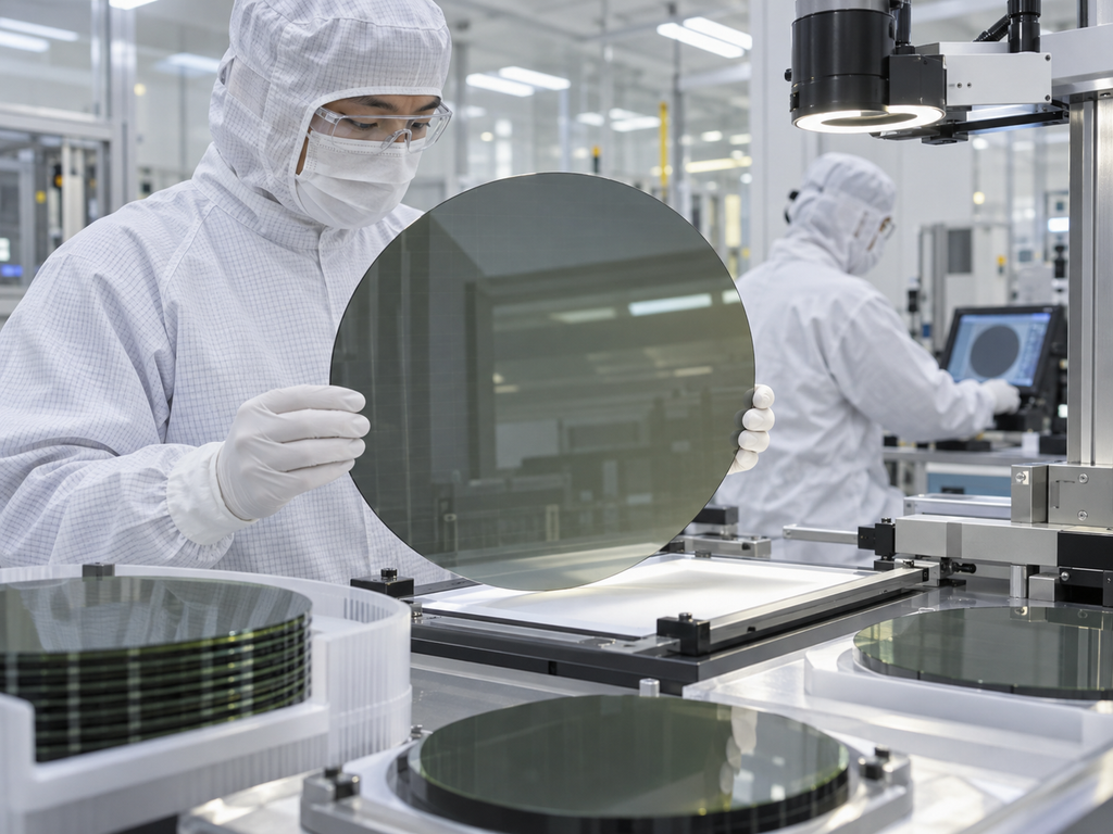
Silicon carbide (SiC) substrates have become one of the most important materials for next-generation power electronics. As electric vehicles, renewable energy systems, industrial drives, rail traction, and AI data center power systems continue to demand higher efficiency and higher voltage operation, the need for larger-diameter SiC wafers is increasing rapidly. After the industry’s transition from 4-inch to 6-inch and then to 8-inch wafers, attention is now shifting toward 300mm (12-inch) SiC substrates. The move to 300mm SiC is not simply a matter of increasing wafer size. It introduces a new level of complexity in crystal growth, wafer shaping, grinding, polishing, defect control, and metrology. Parameters such as total thickness variation […]

300mm (12-Inch) SiC Substrates: Crystal Growth, TTV, Bow, Warp, Defect Control and Challenges for Mass Production 続きを読む »

Why High-NA EUV Raises the Bar for SiC Ceramic Precision Structures: Thermal Drift, Stiffness, Vibration Control and Lightweight Design

High-NA extreme ultraviolet lithography is designed to print smaller semiconductor features with greater imaging contrast. By increasing numerical aperture from 0.33 in conventional EUV systems to 0.55, the technology can resolve substantially finer patterns using the same 13.5 nm EUV wavelength. The ASML TWINSCAN EXE:5000, the first High-NA EUV system, provides 8 nm resolution and can print features approximately 1.7 times smaller than previous NXE systems. Its successor, the EXE:5200B, combines this resolution with improved overlay and productivity. ASML Better optical resolution, however, also creates a more demanding mechanical environment. The wafer, reticle, mirrors and metrology systems must maintain extremely stable relative positions while stages accelerate, structures heat and cool,

Why High-NA EUV Raises the Bar for SiC Ceramic Precision Structures: Thermal Drift, Stiffness, Vibration Control and Lightweight Design 続きを読む »

High-Power Ceramic Substrate Selection Guide: AlN, Si₃N₄ and Alumina for SiC Power Modules

Silicon carbide power devices can operate at higher voltages, switching frequencies and junction temperatures than conventional silicon devices. These advantages support smaller, lighter and more efficient power systems, but they also place greater thermal and mechanical demands on the package. The ceramic substrate is a critical part of this package. It electrically isolates the circuit from the baseplate or heat sink while transferring heat away from the SiC dies. It must also support copper conductors, survive repeated thermal cycling and maintain insulation performance under high voltage. Aluminum nitride, silicon nitride and alumina are three widely considered substrate materials. Each offers a different balance of thermal conductivity, mechanical reliability, dielectric performance,

High-Power Ceramic Substrate Selection Guide: AlN, Si₃N₄ and Alumina for SiC Power Modules 続きを読む »

セラミックウェーハ用エンドエフェクタの設計:材料、重量、平坦度、および粒子管理

A ceramic wafer end effector—also called a wafer handling blade, robot blade or wafer transfer arm—is the part of a semiconductor robot that directly supports and transfers wafers between process chambers, load ports, aligners, inspection stations and wafer carriers. Although its geometry may appear simple, the end effector directly affects wafer positioning accuracy, transfer speed, particle generation, electrostatic discharge risk and equipment uptime. A successful ceramic wafer end effector must combine several requirements: Ceramic end effectors are used because advanced ceramics can provide dimensional precision, thermal stability, abrasion resistance and low-contamination wafer contact. Some wafer-handling systems also use ESD-safe ceramic materials to dissipate accumulated static charge. This guide explains how

セラミックウェーハ用エンドエフェクタの設計:材料、重量、平坦度、および粒子管理 続きを読む »