シンケホイ

How AI Is Reshaping Semiconductor Materials: 300mm Wafers, HBM, SiC and the Next Stage of Competition

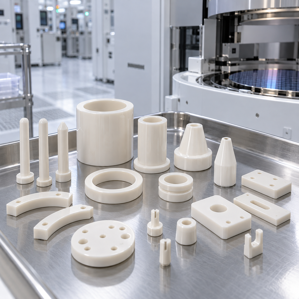
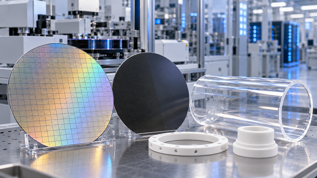
Over the past few years, most discussions about the semiconductor industry have focused on chip design, advanced process nodes and fab expansion. But in 2026, another trend is becoming increasingly clear: The AI boom is moving upstream into semiconductor materials. Silicon wafers, silicon carbide, high-purity quartz, advanced ceramics, carrier wafers and materials used in advanced packaging are becoming more important than ever. The competition is also changing. It is no longer enough for a supplier to simply prove that a material can be manufactured. The real questions are now: For semiconductor materials, the next stage of competition will be increasingly defined by quality, stability and manufacturability. 1. AI Is Driving […]
How AI Is Reshaping Semiconductor Materials: 300mm Wafers, HBM, SiC and the Next Stage of Competition 続きを読む »

Polished Alumina vs AlN Substrates for AI Server Power Modules: Thermal Performance, Flatness and Metallization

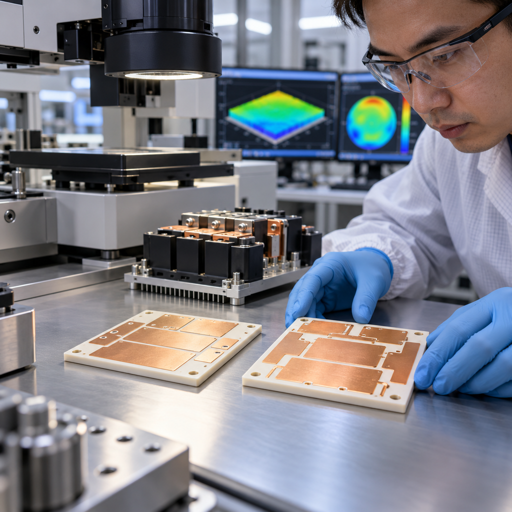
The rapid increase in AI computing density is changing the requirements placed on power conversion hardware. AI servers increasingly require compact, high-efficiency power supplies, DC/DC converters, power stages and advanced thermal-management systems. As power density rises, the ceramic substrate underneath power semiconductor devices becomes increasingly important. Two commonly considered materials are: Both provide electrical insulation, dimensional stability and compatibility with semiconductor packaging processes. However, they behave very differently in terms of: Selecting between polished alumina and AlN should therefore be based on the actual thermal and packaging requirements of the power module rather than material reputation alone. 1. Why Ceramic Substrates Matter More in AI Server Power Systems Power architecture

Polished Alumina vs AlN Substrates for AI Server Power Modules: Thermal Performance, Flatness and Metallization 続きを読む »

Why Do Zirconia Ceramic Parts Crack During Assembly? Fit, Edge Design and Mounting Stress

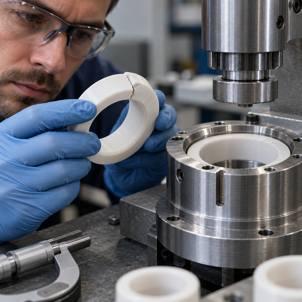
Zirconia ceramics are widely used in precision equipment because of their high hardness, wear resistance, chemical stability and relatively high fracture toughness compared with many other technical ceramics. However, zirconia parts can still crack during assembly. In many cases, the ceramic component itself is not defective. The failure is caused by how the part is designed, fitted, clamped or mounted into a metal or plastic structure. A zirconia sleeve may crack when pressed onto a shaft. A ceramic plate may fracture around a screw hole. A precision ring may split after being installed into a metal housing. Sometimes the component survives assembly but develops delayed cracks after thermal cycling or

Why Do Zirconia Ceramic Parts Crack During Assembly? Fit, Edge Design and Mounting Stress 続きを読む »

SiC Wafer Boat Supplier Qualification: Replacement Fit, Batch Consistency and Acceptance Testing

Qualifying a new SiC wafer boat supplier is very different from simply purchasing a ceramic component according to a drawing. In semiconductor thermal processing, a wafer boat becomes part of the furnace handling and process system. Its slot geometry determines how wafers are supported. Its external dimensions determine whether the boat interfaces correctly with elevators, paddles, transfer mechanisms and other hardware. Its material condition and surface quality can influence particle generation, contamination and long-term stability. For this reason, semiconductor manufacturers looking for an OEM replacement SiC wafer boat, a second-source supplier or a custom furnace boat should evaluate more than price and nominal dimensions. A practical qualification program should answer

SiC Wafer Boat Supplier Qualification: Replacement Fit, Batch Consistency and Acceptance Testing 続きを読む »

300mm Wafer Boat Maintenance and Replacement Guide: Slot Wear, Particle Excursions, Cleaning Windows and End-of-Life Criteria

As semiconductor fabs move more high-volume thermal processes to 300mm wafers, wafer boat condition becomes increasingly important to process stability. A wafer boat may appear to be a simple furnace consumable, but it performs several critical functions at the same time: maintaining wafer spacing, supporting wafers during high-temperature processing, preserving loading accuracy, minimizing contact damage, and avoiding additional particle or metallic contamination. After hundreds or thousands of thermal and loading cycles, however, the condition of a wafer boat gradually changes. Process deposits may accumulate. Wafer slots may wear. Surface roughness can increase. Coatings may deteriorate. Repeated cleaning can alter critical contact areas. Eventually, a boat that still looks usable may

300mm Wafer Boat Maintenance and Replacement Guide: Slot Wear, Particle Excursions, Cleaning Windows and End-of-Life Criteria 続きを読む »

Ceramic Electrostatic Chucks for 300mm Etch and CVD: AlN vs Alumina, Helium Backside Cooling, RF Coupling, Flatness and Particle Control

As plasma etch, PECVD, CVD and other semiconductor processes move toward tighter temperature windows and higher plasma power, the electrostatic chuck has become much more than a wafer-holding component. For 300mm semiconductor equipment, the ceramic electrostatic chuck, or ESC, simultaneously affects wafer clamping, backside helium cooling, RF power delivery, wafer temperature uniformity, particle performance and process repeatability. A poorly matched ESC can cause problems such as local temperature variation, unstable helium pressure, backside particles, wafer sticking, dechuck failure, RF arcing or non-uniform plasma behavior. For equipment manufacturers and replacement-part buyers, selecting an ESC therefore requires more than specifying only the wafer diameter and ceramic material. The ceramic composition, electrode structure,

Ceramic Electrostatic Chucks for 300mm Etch and CVD: AlN vs Alumina, Helium Backside Cooling, RF Coupling, Flatness and Particle Control 続きを読む »

AlN Ceramic Heat Spreaders for AI Optical Engines and CPO: Thermal Conductivity, CTE, Metallization, Flatness and Packaging Reliability

The rapid growth of AI clusters is changing not only processors and networking architectures, but also the materials used inside advanced packages. As electrical links become more difficult to scale at extremely high bandwidths, optical interconnects are moving closer to switch ASICs, accelerators and other high-performance silicon. This transition is driving the development of Co-Packaged Optics (CPO) and increasingly compact optical engines. However, moving photonic devices closer to high-power electronics creates a new problem: heat. Optical engines contain temperature-sensitive components such as lasers, photonic integrated circuits, drivers, transimpedance amplifiers and optical coupling structures. At the same time, nearby ASICs can generate substantial heat. Thermal management therefore becomes a package-level materials

AlN Ceramic Heat Spreaders for AI Optical Engines and CPO: Thermal Conductivity, CTE, Metallization, Flatness and Packaging Reliability 続きを読む »

300mm (12-Inch) SiC Substrates: Crystal Growth, TTV, Bow, Warp, Defect Control and Challenges for Mass Production

Silicon carbide (SiC) substrates have become one of the most important materials for next-generation power electronics. As electric vehicles, renewable energy systems, industrial drives, rail traction, and AI data center power systems continue to demand higher efficiency and higher voltage operation, the need for larger-diameter SiC wafers is increasing rapidly. After the industry’s transition from 4-inch to 6-inch and then to 8-inch wafers, attention is now shifting toward 300mm (12-inch) SiC substrates. The move to 300mm SiC is not simply a matter of increasing wafer size. It introduces a new level of complexity in crystal growth, wafer shaping, grinding, polishing, defect control, and metrology. Parameters such as total thickness variation

300mm (12-Inch) SiC Substrates: Crystal Growth, TTV, Bow, Warp, Defect Control and Challenges for Mass Production 続きを読む »

SiC Wafer Boats for 200mm and 300mm Semiconductor Furnaces: Slot Pitch, Purity, Thermal Shock, Particle Control and Cleaning Requirements

Silicon carbide wafer boats are critical furnace components used to support and position semiconductor wafers during high-temperature batch processes such as oxidation, annealing, diffusion and LPCVD. For 200mm and 300mm wafer processing, the wafer boat is much more than a simple ceramic carrier. Its slot geometry determines wafer positioning. Its dimensional stability influences process uniformity. Its surface condition affects particle generation. Its material purity can influence contamination risk. Its resistance to repeated heating, cooling and chemical cleaning ultimately determines furnace uptime and consumable lifetime. Modern vertical furnace systems may process 50 to 100 wafers in a single batch and operate at temperatures reaching approximately 1200–1250°C depending on the process and

SiC Wafer Boats for 200mm and 300mm Semiconductor Furnaces: Slot Pitch, Purity, Thermal Shock, Particle Control and Cleaning Requirements 続きを読む »

High-Purity Zirconia Ceramic Parts for Semiconductor Equipment: YSZ Purity, Wear Resistance, Surface Finish, Contamination Control and Custom Machining

Semiconductor equipment contains many small mechanical components that rarely attract the same attention as wafer chucks, heaters or process chambers, yet their material quality can directly influence equipment stability and contamination performance. Guide pins, positioning blocks, bushings, sleeves, nozzles, wear pads, insulating spacers, precision shafts and other contact components may operate for millions of cycles while maintaining tight dimensional tolerances. For these applications, yttria-stabilized zirconia, commonly referred to as YSZ, offers an unusual combination of high strength, fracture toughness, wear resistance, electrical insulation and the ability to achieve a very fine surface finish. These characteristics make zirconia attractive for selected semiconductor equipment components, particularly where repeated mechanical contact, low wear

High-Purity Zirconia Ceramic Parts for Semiconductor Equipment: YSZ Purity, Wear Resistance, Surface Finish, Contamination Control and Custom Machining 続きを読む »

Ceramic End Effectors for 200mm and 300mm Wafer Handling: Alumina vs SiC, Flatness, Vacuum Grooves, Particle Control and Robot Compatibility

In semiconductor manufacturing, wafer handling components are often overlooked until they begin to affect yield, uptime or equipment stability. Among these components, the ceramic end effector plays a critical role in transporting wafers safely and repeatably between process stations. As fabs continue to emphasize higher automation, lower particle generation and tighter dimensional control, the performance requirements for wafer handling end effectors are becoming more demanding. This is especially true for 200mm and 300mm wafer lines, where robotic handling must remain stable across thousands or even millions of cycles. Ceramic end effectors are widely used because they offer a combination of rigidity, cleanliness, wear resistance and dimensional stability. However, not all

Ceramic End Effectors for 200mm and 300mm Wafer Handling: Alumina vs SiC, Flatness, Vacuum Grooves, Particle Control and Robot Compatibility 続きを読む »

Why High-NA EUV Raises the Bar for SiC Ceramic Precision Structures: Thermal Drift, Stiffness, Vibration Control and Lightweight Design

High-NA extreme ultraviolet lithography is designed to print smaller semiconductor features with greater imaging contrast. By increasing numerical aperture from 0.33 in conventional EUV systems to 0.55, the technology can resolve substantially finer patterns using the same 13.5 nm EUV wavelength. The ASML TWINSCAN EXE:5000, the first High-NA EUV system, provides 8 nm resolution and can print features approximately 1.7 times smaller than previous NXE systems. Its successor, the EXE:5200B, combines this resolution with improved overlay and productivity. ASML Better optical resolution, however, also creates a more demanding mechanical environment. The wafer, reticle, mirrors and metrology systems must maintain extremely stable relative positions while stages accelerate, structures heat and cool,

Why High-NA EUV Raises the Bar for SiC Ceramic Precision Structures: Thermal Drift, Stiffness, Vibration Control and Lightweight Design 続きを読む »