xinkehui

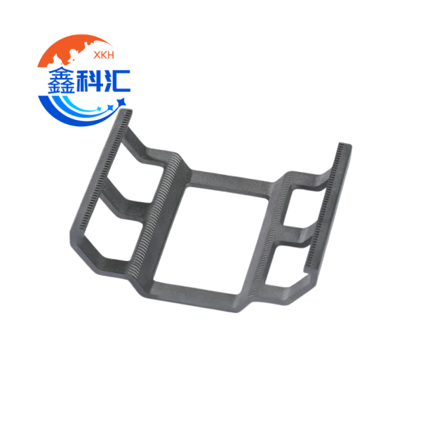
What Is a Semiconductor Wafer Boat? Materials, Structure and Applications

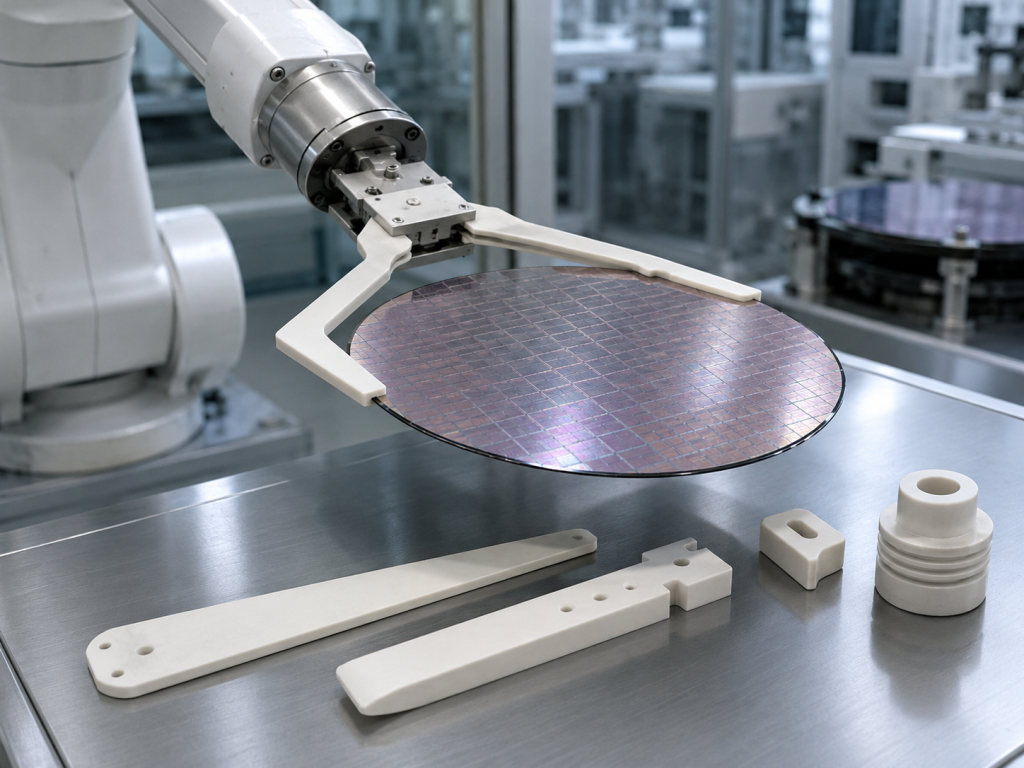
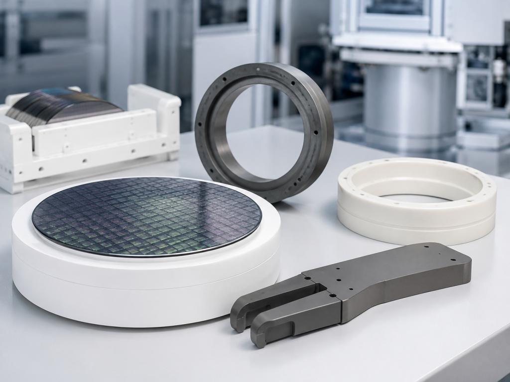
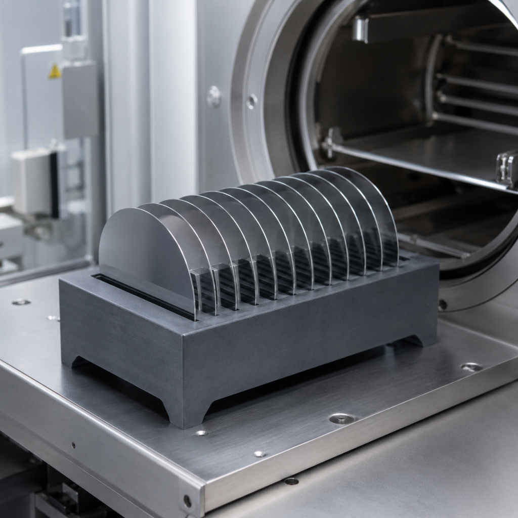
In semiconductor manufacturing, wafers must be processed, transported, heated and cooled under highly controlled conditions. During high-temperature processes such as diffusion, oxidation, annealing and LPCVD, wafers cannot simply be placed directly inside a furnace. They need a stable, clean and precisely designed carrier to hold them in position. This carrier is commonly known as a […]

What Is a Semiconductor Wafer Boat? Materials, Structure and Applications Lire la suite »

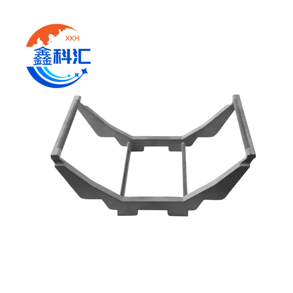
Ceramic Substrates: The Thermal Management Backbone of Advanced Electronic Devices

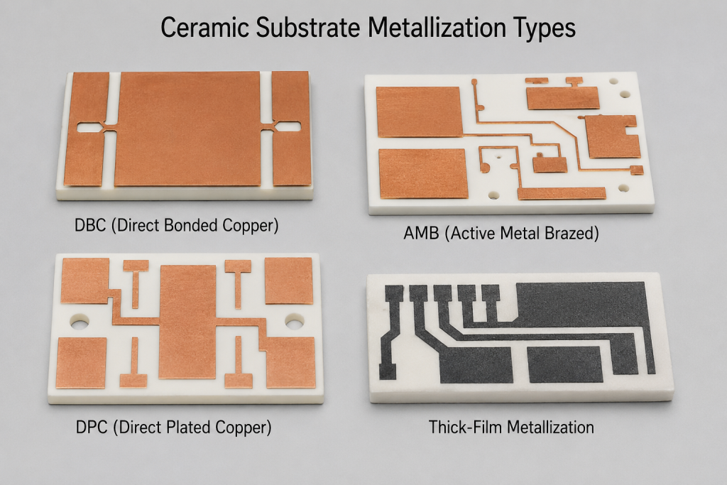
As emerging technologies such as electric vehicles (EVs), 5G communications, renewable energy systems, artificial intelligence (AI), aerospace electronics, and power semiconductors continue to evolve, electronic devices are becoming increasingly powerful, compact, and highly integrated. While these advancements improve performance, they also generate significantly higher heat densities, creating critical challenges for thermal management and device reliability.

Ceramic Substrates: The Thermal Management Backbone of Advanced Electronic Devices Lire la suite »

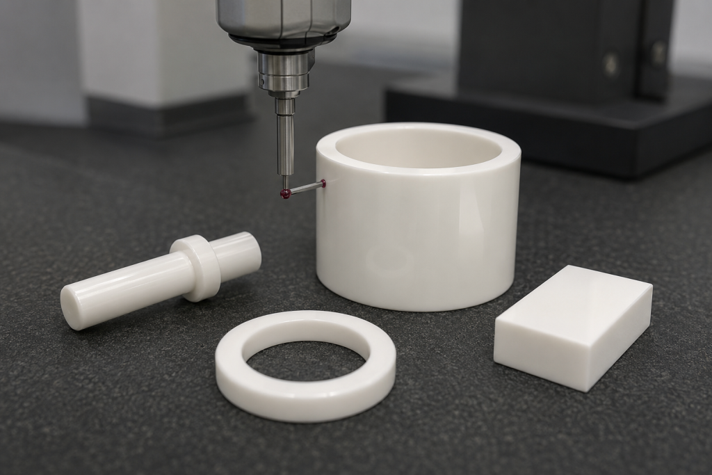
Advanced Ceramic Materials in Semiconductor Optoelectronics: Applications, Advantages, and Future Prospects

As semiconductor and optoelectronic technologies continue to advance toward higher power, greater integration, and improved reliability, the demand for high-performance materials is growing rapidly. Among the many advanced materials used in modern optoelectronic devices, ceramic materials have emerged as a critical enabling technology due to their exceptional thermal stability, chemical resistance, electrical insulation, and optical

Advanced Ceramic Materials in Semiconductor Optoelectronics: Applications, Advantages, and Future Prospects Lire la suite »

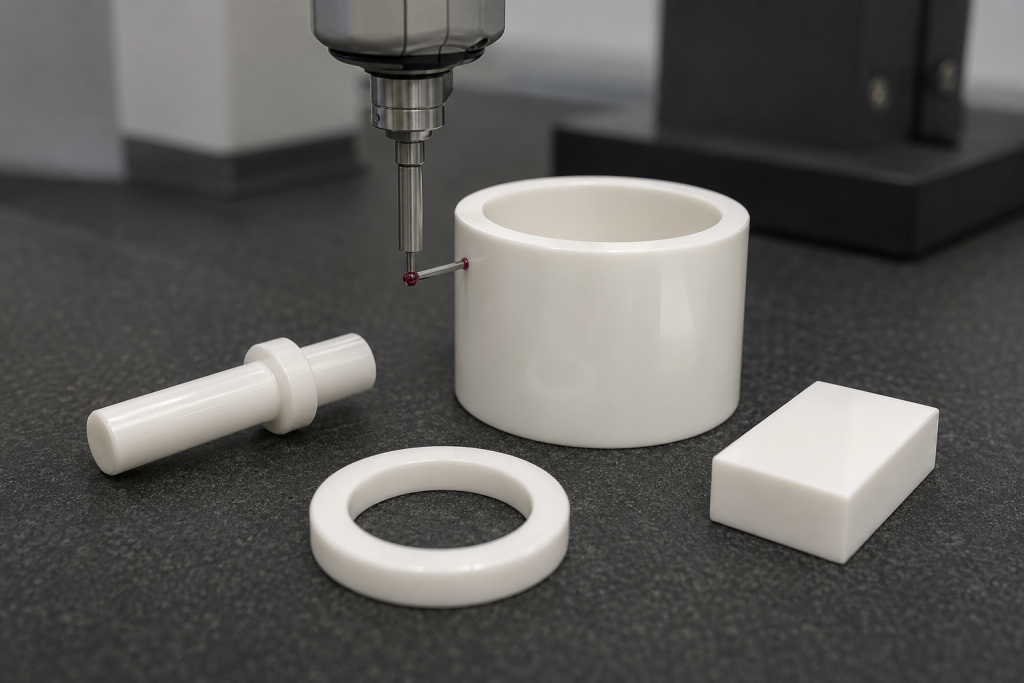
Overcoming the Challenges of Manufacturing Complex Semiconductor Ceramic Components

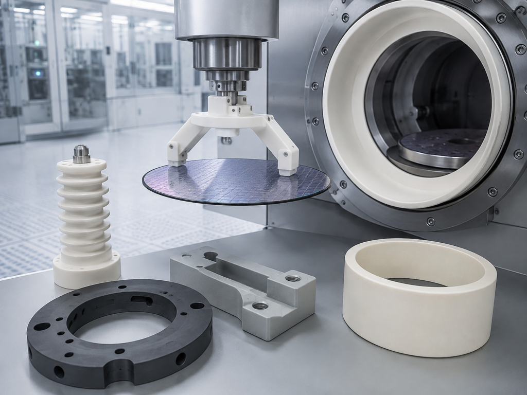
Advanced ceramics have become indispensable materials in modern semiconductor equipment. Components used in plasma etching, chemical vapor deposition (CVD), physical vapor deposition (PVD), ion implantation, and wafer handling systems must operate reliably under extreme conditions, including high-energy plasma exposure, corrosive process gases, elevated temperatures, thermal cycling, and high-voltage electrical fields. Materials such as alumina (Al₂O₃),

Overcoming the Challenges of Manufacturing Complex Semiconductor Ceramic Components Lire la suite »

Les 6 principaux matériaux de substrat céramique expliqués : un guide complet

With the rapid development of electric vehicles, power electronics, aerospace systems, satellite communications, and high-frequency semiconductor devices, electronic components are increasingly required to operate under high power, high temperature, and high frequency conditions. In such demanding environments, traditional organic or metal-based substrates often fail to provide sufficient thermal and electrical stability. As a result, advanced

Les 6 principaux matériaux de substrat céramique expliqués : un guide complet Lire la suite »

Support céramique en carbure de silicium (SiC) poreux : technologie de frittage à basse température et étude des performances

Silicon Carbide (SiC) porous ceramic supports are widely used in advanced membrane filtration systems due to their excellent thermal stability, high mechanical strength, and superior chemical resistance. SiC-based ceramic materials are especially suitable for harsh environments such as high-temperature filtration, wastewater treatment, and chemical processing. However, conventional SiC ceramics require extremely high sintering temperatures (>2000°C),

Support céramique en carbure de silicium (SiC) poreux : technologie de frittage à basse température et étude des performances Lire la suite »

Céramiques au carbure de silicium : matériaux d'ingénierie de pointe pour les environnements industriels extrêmes

As industrial equipment continues to evolve toward higher precision, higher temperatures, and more demanding operating conditions, conventional materials such as metals and standard ceramics are increasingly reaching their performance limits. Wear, thermal deformation, chemical corrosion, particle contamination, and electrical instability can all negatively impact manufacturing efficiency, product quality, and equipment lifespan. Among advanced engineering materials,

Céramiques au carbure de silicium : matériaux d'ingénierie de pointe pour les environnements industriels extrêmes Lire la suite »

Comment hBN favorise le développement des matériaux 2D de nouvelle génération

The rapid expansion of two-dimensional (2D) materials research has opened entirely new directions in electronics, photonics, and quantum technologies. Materials such as graphene, transition metal dichalcogenides (TMDs), and other atomically thin crystals exhibit extraordinary properties that differ fundamentally from their bulk counterparts. However, the practical realization of high-performance 2D devices depends not only on the

Comment hBN favorise le développement des matériaux 2D de nouvelle génération Lire la suite »

Pourquoi le hBN de qualité « device-grade » devient un matériau stratégique pour les futurs semi-conducteurs

As semiconductor technology continues to scale beyond traditional silicon-based architectures, the industry is increasingly turning toward new classes of materials that can support higher performance, lower power consumption, and fundamentally new device physics. Among these emerging materials, device-grade hexagonal boron nitride (hBN) single crystal has rapidly gained attention as a strategic enabler for next-generation electronics.

Pourquoi le hBN de qualité « device-grade » devient un matériau stratégique pour les futurs semi-conducteurs Lire la suite »

Le graphène et le hBN : le partenariat le plus important dans le domaine de l'électronique 2D

Dans le domaine en pleine évolution des matériaux bidimensionnels (2D), peu de combinaisons de matériaux ont eu un impact aussi profond que celui du graphène et du nitrure de bore hexagonal (hBN). Si le graphène est réputé pour ses propriétés électriques, mécaniques et thermiques extraordinaires, son plein potentiel ne peut être exploité qu'en association avec un partenaire tout aussi remarquable : des monocristaux de hBN de haute qualité.

Le graphène et le hBN : le partenariat le plus important dans le domaine de l'électronique 2D Lire la suite »

Pourquoi les dispositifs à base de graphène à haute mobilité reposent sur des monocristaux de hBN

Graphene is widely regarded as one of the most remarkable materials ever discovered. Its exceptional electrical conductivity, mechanical strength, and atomic thickness have opened new possibilities in nanoelectronics, sensing, and quantum technologies. However, one of the most important discoveries in graphene research is that its performance is not solely determined by graphene itself—but critically depends

Pourquoi les dispositifs à base de graphène à haute mobilité reposent sur des monocristaux de hBN Lire la suite »

Qu'est-ce qu'un monocristal de hBN de qualité électronique et pourquoi est-il important pour l'électronique de pointe ?

As the fields of two-dimensional (2D) materials, quantum devices, and next-generation semiconductors continue to evolve, one material has emerged as a critical foundation for many of the most promising technological breakthroughs: Device-Grade Hexagonal Boron Nitride (hBN) Single Crystal. Often referred to as the “ideal companion” to graphene, high-quality hBN has become indispensable in the fabrication

Qu'est-ce qu'un monocristal de hBN de qualité électronique et pourquoi est-il important pour l'électronique de pointe ? Lire la suite »