
Company News

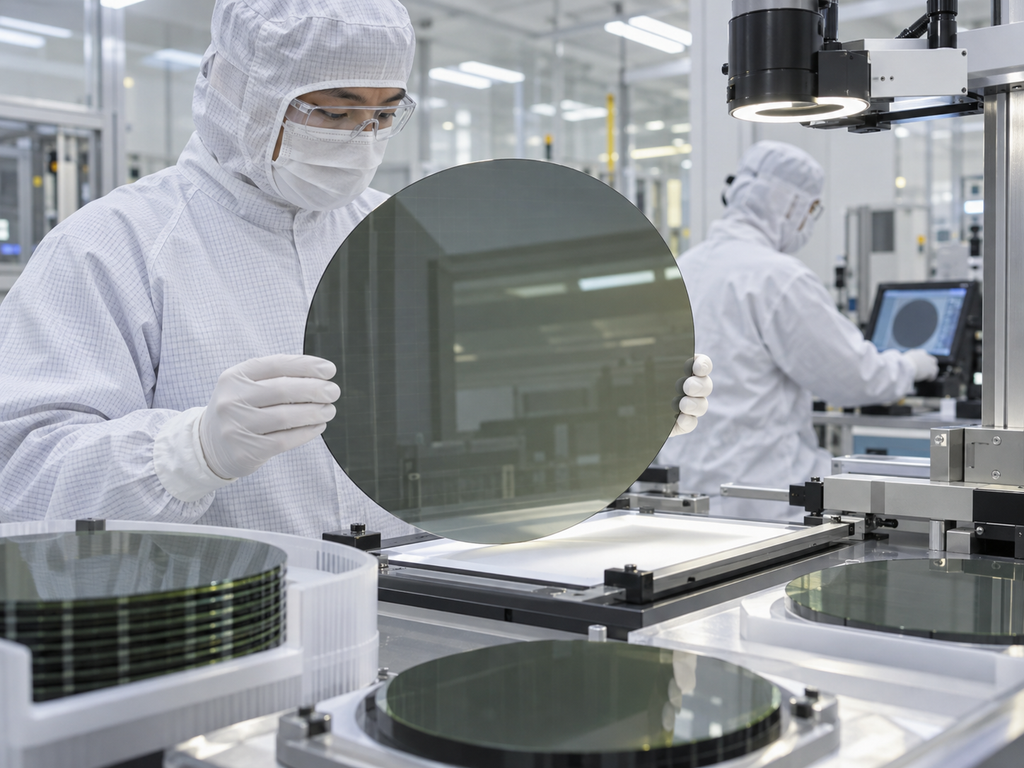
300mm (12-Inch) SiC Substrates: Crystal Growth, TTV, Bow, Warp, Defect Control and Challenges for Mass Production

Silicon carbide (SiC) substrates have become one of the most important materials for next-generation power electronics. As electric vehicles, renewable energy systems, industrial drives, rail traction, and AI data center power systems continue to demand higher efficiency and higher voltage operation, the need for larger-diameter SiC wafers is increasing rapidly. After the industry’s transition from […]

300mm (12-Inch) SiC Substrates: Crystal Growth, TTV, Bow, Warp, Defect Control and Challenges for Mass Production Read More »

Why High-NA EUV Raises the Bar for SiC Ceramic Precision Structures: Thermal Drift, Stiffness, Vibration Control and Lightweight Design

High-NA extreme ultraviolet lithography is designed to print smaller semiconductor features with greater imaging contrast. By increasing numerical aperture from 0.33 in conventional EUV systems to 0.55, the technology can resolve substantially finer patterns using the same 13.5 nm EUV wavelength. The ASML TWINSCAN EXE:5000, the first High-NA EUV system, provides 8 nm resolution and

Why High-NA EUV Raises the Bar for SiC Ceramic Precision Structures: Thermal Drift, Stiffness, Vibration Control and Lightweight Design Read More »

High-Power Ceramic Substrate Selection Guide: AlN, Si₃N₄ and Alumina for SiC Power Modules

Silicon carbide power devices can operate at higher voltages, switching frequencies and junction temperatures than conventional silicon devices. These advantages support smaller, lighter and more efficient power systems, but they also place greater thermal and mechanical demands on the package. The ceramic substrate is a critical part of this package. It electrically isolates the circuit

High-Power Ceramic Substrate Selection Guide: AlN, Si₃N₄ and Alumina for SiC Power Modules Read More »

Ceramic Wafer End Effector Design: Material, Weight, Flatness and Particle Control

A ceramic wafer end effector—also called a wafer handling blade, robot blade or wafer transfer arm—is the part of a semiconductor robot that directly supports and transfers wafers between process chambers, load ports, aligners, inspection stations and wafer carriers. Although its geometry may appear simple, the end effector directly affects wafer positioning accuracy, transfer speed,

Ceramic Wafer End Effector Design: Material, Weight, Flatness and Particle Control Read More »