
When people think about the semiconductor industry, they usually focus on chips, wafers, or advanced process nodes. However, behind every semiconductor breakthrough lies a less visible but equally critical foundation: advanced materials.
As semiconductor manufacturing continues to pursue higher precision, smaller geometries, and faster production speeds, equipment performance requirements are becoming increasingly demanding. This shift is creating new opportunities for advanced engineering materials—especially Silicon Carbide (SiC) ceramics.
From lithography machines to wafer processing systems, silicon carbide ceramics are rapidly becoming key components in modern semiconductor equipment. Once considered a niche material, SiC ceramics are now helping build what many industry experts see as a future multi-billion-dollar market.
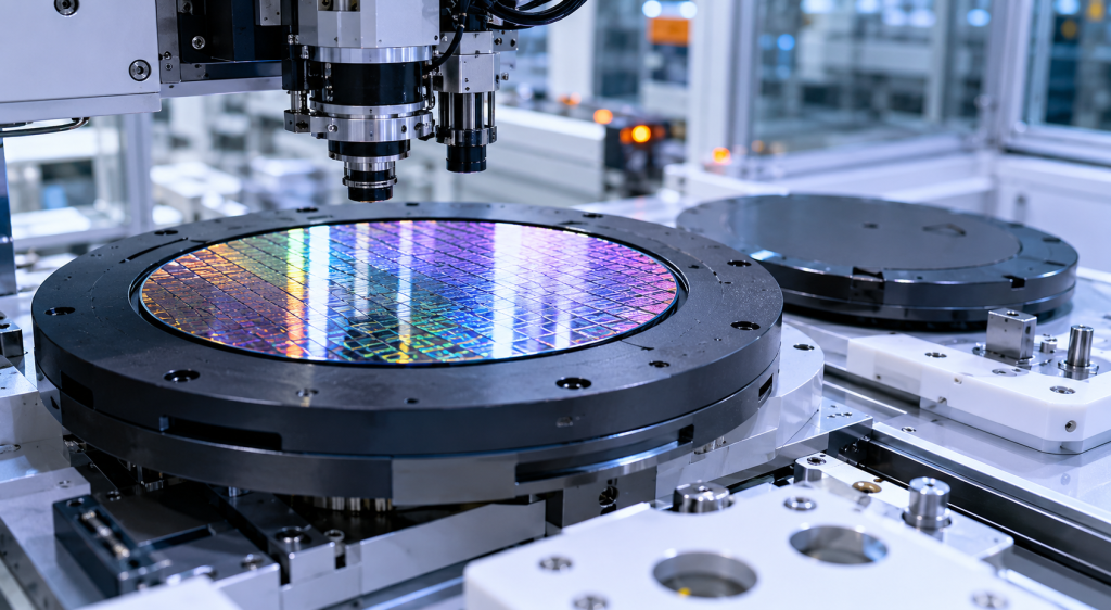
The Hidden Material Behind Semiconductor Manufacturing
Semiconductor fabrication involves far more than simply producing chips. A modern wafer fabrication process includes:
- Lithography
- Etching
- Thin-film deposition
- Thermal processing
- Cleaning
- Chemical mechanical polishing (CMP)
These manufacturing environments expose equipment components to:
- High temperatures
- Vacuum conditions
- Corrosive gases
- Plasma environments
- High-speed precision motion
Even minor thermal deformation, mechanical wear, or particle contamination can negatively impact wafer yield and production efficiency.
As a result, material selection has become increasingly important in semiconductor equipment design.
Among various advanced materials, silicon carbide ceramics have emerged as a preferred choice.
Why Silicon Carbide Ceramics?
Compared with traditional metals and conventional ceramics, silicon carbide offers an exceptional combination of mechanical, thermal, and chemical properties.
Key advantages include:
- Extremely high hardness
- Outstanding wear resistance
- Low thermal expansion coefficient
- Excellent thermal conductivity
- Superior high-temperature stability
- High stiffness with lightweight potential
- Strong corrosion and oxidation resistance
- Low particle generation
These properties allow semiconductor equipment to maintain precision and reliability under demanding operating conditions.
As process technologies continue to evolve, material performance is becoming a critical factor in determining equipment capability.
Silicon Carbide Plays a Critical Role in Lithography Systems
Lithography equipment is widely considered one of the most sophisticated machines in semiconductor manufacturing.
Advanced lithography stages require:
- Nanometer-level positioning accuracy
- High acceleration movement
- Low vibration performance
- Long-term dimensional stability
Traditional structural materials may suffer from thermal deformation and stiffness limitations during high-speed operation.
Silicon carbide ceramics provide an attractive alternative because they combine:
- Lightweight construction
- High rigidity
- Fast response capability
- Excellent dimensional stability
As a result, SiC components are increasingly used in:
- Precision stages
- Guide rails
- Mirrors
- Ceramic vacuum chucks
- Structural support systems
- Optical mechanical assemblies
Although these parts are often invisible to end users, they directly affect machine performance and manufacturing accuracy.
Beyond Lithography: SiC Is Expanding Across Wafer Manufacturing
Silicon carbide ceramics are no longer limited to high-end lithography equipment. They are becoming increasingly common throughout semiconductor fabrication systems.
Wafer Fixtures and Carrier Components
Semiconductor wafers undergo multiple thermal processes such as:
- Oxidation
- Diffusion
- Annealing
- CVD processing
- Heat treatment
Equipment components must maintain dimensional stability under repeated thermal cycling.
Silicon carbide carrier structures offer:
- High thermal shock resistance
- Excellent mechanical stability
- Reduced contamination risk
- Long operating life
These benefits make them ideal for high-temperature processing applications.
Precision Grinding and Polishing Systems
Wafer polishing requires extremely tight flatness control.
Traditional metal polishing plates often experience:
- Rapid wear
- Thermal expansion
- Reduced precision over time
Silicon carbide grinding components offer:
- Higher hardness
- Lower wear rates
- Better thermal matching with silicon wafers
- Improved process consistency
This contributes to higher wafer quality and improved production yield.
Etching and Thin-Film Deposition Equipment
Etching and deposition chambers operate under highly aggressive conditions.
Components are exposed to:
- Reactive plasma
- Corrosive gases
- High temperatures
- Vacuum environments
Silicon carbide ceramics are increasingly used for:
- Focus rings
- Susceptors
- Chamber parts
- Structural assemblies
Their resistance to plasma erosion and chemical attack helps improve equipment reliability and reduce particle contamination.
A Rapidly Growing Market Opportunity
As semiconductor investments continue to rise globally, demand for advanced ceramic components is expanding rapidly.
Several key trends are driving market growth:
Semiconductor Capacity Expansion
The rapid development of:
- Artificial intelligence chips
- Automotive electronics
- Power semiconductors
- Data centers
- Advanced memory technologies
is fueling demand for new semiconductor fabs and manufacturing equipment.
Every new production line creates demand for high-performance structural materials.
Semiconductor Equipment Localization
Many countries and regions are accelerating domestic semiconductor supply chain development.
This trend creates new opportunities for advanced ceramic manufacturers capable of supplying precision semiconductor components.
Increasing Equipment Complexity
As semiconductor technology advances, equipment requires:
- Higher precision
- Lower contamination
- Better dimensional stability
- Lightweight structures
These requirements align closely with the strengths of silicon carbide ceramics.
Future Development Trends for Silicon Carbide Ceramics
The next phase of SiC development will likely focus on:
Larger integrated structures
Supporting advanced lithography and precision platforms.
Lightweight hollow designs
Reducing moving mass while maintaining stiffness.
Ultra-high purity materials
Minimizing contamination risks.
Advanced surface engineering
Improving coatings and surface performance.
Customized semiconductor solutions
Providing application-specific component designs.
Manufacturers that master large-scale, high-purity, and precision SiC fabrication technologies may gain significant advantages in the future semiconductor market.
Conclusion
As semiconductor manufacturing evolves, competition is no longer limited to chips and process technologies. Equipment materials are becoming equally important.
From lithography systems to wafer manufacturing, silicon carbide ceramics are steadily expanding their role throughout semiconductor production.
What once appeared to be a specialized engineering material is now emerging as a key enabler of next-generation semiconductor equipment—and potentially a major growth market for years to come.
FAQ
Why are silicon carbide ceramics used in semiconductor equipment?
Silicon carbide ceramics provide high stiffness, thermal stability, corrosion resistance, and low particle generation, making them ideal for precision semiconductor manufacturing.
What semiconductor components commonly use SiC ceramics?
Common applications include wafer chucks, wafer boats, guide rails, precision stages, mirrors, focus rings, and process chamber components.
Can silicon carbide ceramic parts be customized?
Yes. Semiconductor-grade SiC components can be customized in terms of dimensions, geometries, coatings, and surface finishes.
Is demand for SiC ceramics expected to grow?
Yes. As semiconductor production expands and equipment becomes more advanced, demand for high-performance ceramic materials is expected to increase significantly.

