
Semiconductor equipment contains many small mechanical components that rarely attract the same attention as wafer chucks, heaters or process chambers, yet their material quality can directly influence equipment stability and contamination performance.
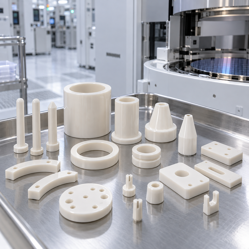
Guide pins, positioning blocks, bushings, sleeves, nozzles, wear pads, insulating spacers, precision shafts and other contact components may operate for millions of cycles while maintaining tight dimensional tolerances.
For these applications, yttria-stabilized zirconia, commonly referred to as YSZ, offers an unusual combination of high strength, fracture toughness, wear resistance, electrical insulation and the ability to achieve a very fine surface finish.
These characteristics make zirconia attractive for selected semiconductor equipment components, particularly where repeated mechanical contact, low wear and precision motion are more important than high thermal conductivity.
However, selecting a zirconia ceramic part for semiconductor equipment requires more than specifying:
“ZrO₂ ceramic.”
Material formulation, stabilizer content, trace impurities, microstructure, surface finish, grinding quality, dimensional tolerance and final cleaning can all influence the actual performance of the finished component.
This article explains the key specifications engineers and buyers should consider when sourcing high-purity zirconia ceramic parts for semiconductor manufacturing equipment.
What Is YSZ Zirconia?
Pure zirconium dioxide, or ZrO₂, undergoes crystallographic phase transformations as temperature changes.
These transformations can generate significant volume changes and make unstabilized zirconia unsuitable for many precision engineering applications.
To control the crystal structure, stabilizing oxides are added.
Yttrium oxide, Y₂O₃, is one of the most widely used stabilizers.
The resulting material is known as:
Yttria-Stabilized Zirconia — YSZ
Depending on composition and processing, zirconia may contain tetragonal, cubic and monoclinic phases in different proportions.
For precision mechanical components, yttria-stabilized tetragonal zirconia polycrystal, often abbreviated Y-TZP or YTZP, is especially important.
Its fine-grained microstructure provides a combination of strength, toughness and wear resistance that is difficult to achieve with many conventional ceramics.
Commercial YTZP grades can exhibit very high mechanical strength and fracture toughness while still allowing submicron-class surface finishes.
Why Zirconia Is Used in Semiconductor Equipment
Semiconductor manufacturing requires components that can maintain dimensional accuracy while minimizing contamination.
Depending on the process tool, ceramic parts may be exposed to:
- repeated sliding or contact
- vacuum environments
- cleaning chemicals
- mechanical impact
- precision positioning
- high-cycle motion
- wafer handling
- assembly and test operations
Zirconia is particularly attractive when mechanical wear and toughness are important.
Its major characteristics include:
- high fracture toughness
- high mechanical strength
- excellent wear resistance
- good corrosion resistance
- electrical insulation
- smooth polishability
- high density
- relatively low thermal conductivity
- good dimensional stability
Compared with more brittle ceramic materials, properly formulated zirconia can tolerate higher mechanical stress and repeated contact.
This makes it useful for components that behave more like precision mechanical parts than furnace or high-temperature structural parts.
Typical Semiconductor Applications
High-purity zirconia components may be used in several areas of semiconductor equipment.
Possible applications include:
- wafer positioning pins
- guide pins
- alignment components
- precision bushings
- sleeves
- ceramic shafts
- wear plates
- mechanical stops
- insulating spacers
- precision nozzles
- pump and fluid-handling components
- wafer handling mechanisms
- semiconductor packaging equipment
- die bonding equipment
- test and assembly systems
- precision metrology fixtures
The suitability of zirconia should always be evaluated against the actual process environment.
A zirconia guide pin in an assembly machine and a ceramic component directly exposed to aggressive plasma have very different material requirements.
YSZ Purity: What Does “High Purity” Actually Mean?
This is one of the most important purchasing questions.
For alumina, buyers often describe purity using values such as:
99.5% Al₂O₃
or
99.9% Al₂O₃.
YSZ requires a more careful definition because yttria is intentionally added to zirconia.
A properly formulated YSZ material may contain:
ZrO₂ + HfO₂
plus a controlled quantity of:
Y₂O₃.
Therefore, simply requesting:
“99.9% ZrO₂”
may not correctly describe the desired material.
Instead, semiconductor buyers should distinguish between:
Main ceramic composition
The intended ZrO₂/Y₂O₃ formulation.
Stabilizer concentration
The controlled amount of yttria required to achieve the desired zirconia phase structure.
Unwanted trace impurities
Elements that are not part of the intended formulation.
For semiconductor applications, these unwanted impurities may be more important than the headline ZrO₂ percentage.
Trace Metal Contamination
Potential contaminating elements can include:
- Fe
- Ni
- Cr
- Cu
- Na
- K
- Ca
- Mg
- Ti
- other transition metals
- alkali metals
The importance of each element depends on where the component is installed.
A component inside a highly contamination-sensitive wafer process may require considerably tighter control than a component used in back-end packaging equipment.
High-purity ceramic components used in semiconductor processing are specifically designed to minimize potential wafer contamination, particularly from transition metals and alkali metals.
For critical projects, buyers should therefore request actual impurity data rather than relying only on a general description such as:
“semiconductor grade.”
3Y-TZP and Other YSZ Compositions
One commonly used engineering zirconia is approximately 3 mol% yttria-stabilized tetragonal zirconia, often called:
3Y-TZP
This composition is widely valued for its excellent combination of:
strength,
fracture toughness,
wear resistance,
and precision machinability after sintering by diamond grinding.
Other yttria concentrations can create different phase structures and material behavior.
A higher yttria content does not automatically mean better mechanical performance.
The correct Y₂O₃ content depends on whether the application prioritizes:
- mechanical toughness
- ionic conductivity
- thermal stability
- phase stability
- wear resistance
For most mechanical semiconductor components, the material grade should be selected according to actual mechanical requirements rather than simply maximizing yttria content.
Why Zirconia Has High Fracture Toughness
One of zirconia’s most valuable properties is transformation toughening.
When a crack begins to propagate through certain zirconia microstructures, tetragonal zirconia grains near the crack tip can transform toward the monoclinic phase.
This transformation involves a local volume expansion.
The expansion creates compressive stress around the crack and can slow further crack propagation.
This mechanism gives zirconia significantly greater fracture toughness than many conventional structural ceramics.
CoorsTek describes this transformation-toughening behavior as one of the reasons zirconia combines high strength with strong resistance to crack propagation and mechanical wear.
For semiconductor equipment, this can be valuable in small precision parts that experience:
repeated contact,
mechanical loading,
impact,
or stress concentration.
Wear Resistance and Particle Generation
Wear resistance is closely linked to contamination control.
Consider a ceramic positioning pin operating continuously inside automated equipment.
Every contact cycle can produce microscopic wear.
If the material wears too quickly, the consequences may include:
dimensional drift,
surface damage,
particles,
unstable positioning,
and increased maintenance frequency.
Zirconia’s high hardness, toughness and fine-grained structure allow it to perform well in many repeated-contact applications.
High-quality YSZ is also used in precision grinding applications specifically because its wear resistance and smooth surface help reduce contamination generated through material wear.
The same general principle is important for semiconductor mechanical components.
However, particle performance depends on much more than the base material.
What Causes Particles from Zirconia Parts?
Typical sources include:
Poor surface grinding
Deep grinding marks may act as initiation points for wear.
Sharp edges
Unsupported sharp ceramic edges can develop microscopic chipping.
Internal porosity
Insufficiently dense material may release grains from the surface.
Poor microstructure
Abnormally large grains or defects can reduce local strength.
Improper cleaning
Residual grinding abrasive or polishing slurry may remain on the part.
Mechanical misalignment
A correctly manufactured ceramic part can still generate particles if installed under excessive contact pressure.
Surface microcracks
Aggressive grinding can introduce subsurface damage that later develops into local chipping.
Therefore, low-particle performance should be treated as a combination of:
material + machining + surface finishing + cleaning + equipment design.
Density and Microstructure Matter
Two zirconia parts with the same nominal chemical composition may perform differently.
Important microstructural factors include:
- sintered density
- grain size
- pore distribution
- phase composition
- secondary phases
- inclusion content
- sintering uniformity
For precision semiconductor equipment components, high density is usually desirable because pores can reduce mechanical strength and create locations where contaminants accumulate.
Fine and uniform grain structures can also improve:
surface quality,
mechanical consistency,
and wear behavior.
This is why raw material control and sintering quality matter even when the final dimensions are produced through CNC grinding.
Surface Finish Is a Functional Specification
Surface roughness is not simply a cosmetic requirement.
For semiconductor equipment components, surface condition can affect:
- friction
- wear
- particle generation
- vacuum sealing
- positioning repeatability
- cleanability
- contact stress
Zirconia has an important advantage in this area because high-quality YTZP materials can achieve very smooth finishes, including submicron-scale surfaces.
But the required surface roughness should depend on the functional area.
A polished shaft may need a different finish from:
a mounting surface,
a ceramic nozzle,
a locating pin,
or a non-contact exterior surface.
How to Specify Surface Roughness
Instead of requesting:
“highly polished”
the RFQ should specify a measurable requirement such as:
Ra ≤ customer-specified value
or
Ra / Rz according to the drawing.
The measurement method should also be agreed.
Important details include:
- contact profilometer or optical method
- measurement direction
- cutoff length
- evaluation length
- polished area
- whether the requirement applies to all surfaces or only critical surfaces
For extremely smooth surfaces, different metrology methods can produce different results.
Therefore, supplier and customer should agree on the inspection method before production.
Polished Surface vs Precision Ground Surface
Not every zirconia component needs polishing.
Precision ground surfaces
May be appropriate for:
- mounting features
- dimensional datums
- external geometry
- non-sliding precision surfaces
Polished surfaces
May be beneficial for:
- sliding contact
- sealing
- precision shafts
- wear surfaces
- wafer-adjacent components
- particle-sensitive contact areas
Over-specifying polishing increases cost.
The correct approach is to identify the surfaces that actually influence equipment performance.
Surface Finish and Contamination Are Connected
A rougher surface has more microscopic peaks, valleys and potential particle-trapping areas.
It may be more difficult to clean completely.
A carefully finished surface can reduce:
mechanical abrasion,
material retention,
cleaning residue,
and local particle shedding.
But extremely low Ra alone does not guarantee semiconductor cleanliness.
A mirror-like surface can still be contaminated by:
metallic grinding residues,
polishing compounds,
organic residues,
or improper packaging.
Therefore:
surface roughness and surface cleanliness must be specified separately.
Precision Grinding of Zirconia
Fully sintered zirconia is extremely hard.
Conventional metal machining tools cannot efficiently machine finished zirconia.
Final precision processing generally requires diamond tooling and processes such as:
- diamond grinding
- ID/OD grinding
- surface grinding
- centerless grinding
- CNC ceramic grinding
- lapping
- polishing
- ultrasonic-assisted machining where appropriate
- laser processing for selected geometries
Many parts are shaped before sintering and then finish-ground after sintering.
The manufacturing route depends on:
geometry,
tolerance,
quantity,
surface finish,
and cost.
Why Sintering Shrinkage Matters
Ceramic parts shrink during sintering.
Unlike CNC machining a metal block, a ceramic manufacturer must account for dimensional change between the green body and the finished dense ceramic.
This means high-precision ceramic manufacturing normally involves two stages.
Near-net-shape forming
The part is initially produced oversized.
Post-sintering machining
Critical dimensions are diamond ground to final tolerance.
For simple high-volume components, manufacturers may optimize tooling to reduce post-machining.
For complex semiconductor equipment parts, however, precision grinding remains important.
What Tolerances Are Possible?
There is no single tolerance that applies to every zirconia component.
Achievable tolerance depends strongly on:
- part length
- wall thickness
- hole diameter
- aspect ratio
- geometry
- grinding access
- flatness
- concentricity
- required surface finish
Typical semiconductor drawings may require control over:
- dimensional tolerance
- flatness
- parallelism
- perpendicularity
- roundness
- cylindricity
- concentricity
- position tolerance
The correct tolerance should be defined by equipment function rather than making every dimension unnecessarily tight.
Flatness
For ceramic plates, guides and support components, flatness can be particularly important.
Poor flatness may affect:
- assembly alignment
- motion accuracy
- sealing
- contact pressure
- wafer positioning
Flatness must be considered together with:
part thickness,
overall length,
sintering stress,
and final grinding method.
A thin zirconia plate with large dimensions may be much more difficult to manufacture than a compact block with the same nominal flatness specification.
Precision Holes and Small Features
Semiconductor ceramic components often contain:
- precision holes
- slots
- narrow grooves
- countersinks
- stepped holes
- thin ribs
- internal channels
These features can significantly increase machining difficulty.
Particularly important factors include:
minimum hole diameter,
hole depth,
aspect ratio,
distance from the hole to the edge,
and tolerance.
A design that is easy in stainless steel may be unnecessarily difficult or fragile when transferred directly to ceramic.
For custom zirconia components, early design-for-manufacturing review can reduce cost and breakage risk.
Edge Chipping Control
Because zirconia is a ceramic, edge condition requires special attention.
Although zirconia is tougher than many ceramics, unsupported sharp corners can still chip during:
machining,
cleaning,
assembly,
shipping,
or repeated mechanical contact.
Where function allows, designers may use:
small chamfers,
controlled radii,
or edge breaks
to reduce stress concentration.
For semiconductor parts, edge finishing can also reduce particle-generation risk.
The engineering drawing should clearly define which edges must remain sharp and which can be chamfered.
Contamination Control During Machining
Using high-purity raw material is not enough.
Contamination can be introduced during manufacturing.
Potential contamination sources include:
- grinding wheels
- metallic fixtures
- coolant
- cutting fluid
- polishing slurry
- operator handling
- cleaning equipment
- packaging materials
For semiconductor-grade components, manufacturing and cleaning procedures should be designed to prevent the final surface from acquiring contaminants after sintering.
This is particularly important when trace-metal control is more stringent than ordinary industrial ceramic requirements.
Final Cleaning
After machining, zirconia parts may require application-specific cleaning.
The process can involve combinations of:
- ultrasonic cleaning
- DI water rinsing
- chemistry-specific cleaning
- filtered drying
- cleanroom inspection
- clean packaging
The exact procedure depends on how the component will be used.
A part supplied for semiconductor packaging equipment may not need the same cleanliness protocol as a component installed close to a wafer-processing chamber.
Therefore, the buyer should specify the required cleanliness level instead of simply asking for “cleanroom cleaning.”
Packaging Matters
A precision-cleaned ceramic component can be contaminated again during packaging and transport.
For sensitive semiconductor applications, packaging considerations may include:
- clean polyethylene bags
- double bagging
- controlled cleanroom packaging
- protective trays
- individual separation between parts
- prevention of ceramic-to-ceramic contact
- lot identification
Heavy zirconia parts can damage each other if they are allowed to collide during transportation.
Proper packaging protects both cleanliness and dimensional integrity.
Can Zirconia Be Used in Plasma Chambers?
This requires careful application review.
Zirconia can provide useful mechanical and chemical properties, but not every zirconia composition is the optimum material for direct exposure to aggressive semiconductor plasma.
In highly corrosive fluorine- or chlorine-containing plasma environments, materials such as high-purity yttria or specially engineered plasma-resistant ceramics and coatings may be preferred.
Yttria-containing surfaces are widely used in semiconductor plasma processing because they can provide resistance to plasma erosion while reducing particle and contamination risks.
Therefore, buyers should clearly distinguish between:
mechanical zirconia parts used inside semiconductor equipment
and
direct plasma-facing chamber components.
A YSZ mechanical guide that performs very well in a transfer module should not automatically be assumed to be the correct material for an etch chamber liner.
Zirconia vs Alumina for Semiconductor Equipment
Alumina and zirconia overlap in many applications, but they have different strengths.
Zirconia
Typically provides:
- higher fracture toughness
- higher mechanical strength
- excellent wear resistance
- smoother achievable surface
- better resistance to mechanical impact
Alumina
Typically provides:
- lower material cost
- wider semiconductor industry usage
- good electrical insulation
- good chemical resistance
- higher-temperature capability for many grades
- easier sourcing in high-purity compositions
For wear-intensive mechanical parts, zirconia often becomes attractive.
For general insulating structural components, high-purity alumina may be more economical.
Zirconia vs Silicon Carbide
SiC is very different from zirconia.
Silicon carbide provides:
- very high stiffness
- high hardness
- high thermal conductivity
- excellent dimensional stability
- strong semiconductor equipment compatibility
Zirconia provides:
- considerably higher fracture toughness
- strong resistance to mechanical damage
- excellent wear performance
- very fine surface finishing capability
- electrical insulation
For a precision wear pin or bushing, zirconia may be attractive.
For a lightweight, highly rigid 300mm wafer-handling arm or high-temperature structural component, SiC may be more appropriate.
The correct material depends on the failure mechanism the designer is trying to prevent.
Zirconia vs Silicon Nitride
Silicon nitride combines:
high toughness,
high strength,
low density,
and excellent thermal shock resistance.
It is particularly useful for dynamic mechanical applications.
Zirconia is much denser, but can provide exceptional wear resistance and excellent polishing behavior.
If low moving mass is important, Si₃N₄ may have an advantage.
If high surface finish and wear resistance dominate, YSZ may be attractive.
Where High-Purity YSZ Adds the Most Value
YSZ is especially interesting when several conditions occur together:
- repeated contact
- high wear
- precision positioning
- electrical insulation
- particle sensitivity
- smooth surfaces
- tight dimensional tolerances
Examples might include:
precision guide components,
wear interfaces,
positioning pins,
ceramic sleeves,
and assembly/test equipment components.
In these cases, replacing a metal component with ceramic may also eliminate certain metallic wear products.
However, the entire tribological system must still be evaluated.
A zirconia component sliding against another ceramic can behave differently from zirconia operating against stainless steel or polymer.
Custom Machining from Customer Drawings
Most semiconductor equipment ceramic parts are not standard catalog components.
They are manufactured according to:
2D drawings,
3D models,
or existing samples.
A ceramic supplier should therefore review more than dimensions.
Important questions include:
What does the part contact?
Does it slide or rotate?
Does it operate in vacuum?
Is it close to the wafer?
What temperature does it experience?
What chemicals are present?
Which dimensions are functional?
Which surfaces need polishing?
What contamination limits apply?
What is the expected service life?
These questions help determine whether YSZ is appropriate and how the part should be manufactured.
Recommended RFQ Parameters
A useful inquiry for high-purity zirconia semiconductor parts should include the following information.
Material
Material: YSZ / Y-TZP / specified zirconia grade
Required Y₂O₃ content if known
Material purity requirement
Trace impurity limits if critical
Color requirement if relevant
Density requirement if applicable
Application
Semiconductor process or equipment type
Operating environment
Vacuum or atmospheric operation
Mechanical contact condition
Operating temperature
Chemical exposure
Plasma exposure if applicable
Dimensions
2D drawing
3D STEP file if available
Critical dimensions
Dimensional tolerances
Hole tolerances
Flatness
Parallelism
Perpendicularity
Concentricity
Surface
Required Ra
Required polished areas
Ground areas
Edge chamfers
Edge-chip limitations
Scratch requirements
Cleanliness
Particle requirement
Metal contamination requirement
Cleaning method if specified
Cleanroom packaging requirement
Inspection
Dimensional inspection report
CMM report if required
Surface roughness report
Material certificate
Chemical composition report
Density report
Lot traceability
Commercial Information
Prototype quantity
Annual quantity
Replacement frequency
Required delivery schedule
This information allows the ceramic manufacturer to determine the appropriate raw material, forming process, machining route and inspection method.
Example RFQ
A practical inquiry might look like this:
Product: Precision YSZ ceramic guide pin
Application: Semiconductor wafer handling equipment
Material: High-purity yttria-stabilized zirconia
Quantity: 20 pcs prototype, 500 pcs/year estimated
Dimensions: According to drawing
Critical diameter tolerance: According to customer drawing
Straightness: Specified
Surface: Polished contact area
Surface roughness: Customer-specified Ra
Edge: No visible chipping
Environment: Cleanroom, repeated mechanical contact
Inspection: Full dimensional report for first article
Documentation: Material certificate and inspection report
Packaging: Individually protected clean packaging
This is far more useful than simply sending:
“Please quote zirconia ceramic parts.”
Common Purchasing Mistakes
Several mistakes frequently occur when sourcing zirconia semiconductor components.
Mistake 1: Specifying only “ZrO₂”
Different zirconia formulations have different properties.
Specify the intended stabilized zirconia grade.
Mistake 2: Using purity as the only quality indicator
A high nominal ZrO₂ percentage does not describe:
microstructure,
density,
wear resistance,
or trace impurities.
Mistake 3: Making every tolerance extremely tight
Ceramic machining cost rises rapidly as tolerance becomes tighter.
Specify tight tolerances only where function requires them.
Mistake 4: Ignoring edge design
Sharp ceramic corners can become chip sources.
Mistake 5: Specifying Ra but not cleanliness
Surface roughness does not measure metallic or particle contamination.
Mistake 6: Selecting zirconia for every plasma application
Direct plasma-facing components require chemistry-specific material selection.
Mistake 7: Ignoring production repeatability
One successful prototype does not prove stable production capability.
Prototype Qualification Before Volume Production
For critical equipment parts, qualification should normally begin with a small prototype batch.
Evaluation can include:
- dimensional measurement
- assembly test
- surface inspection
- vacuum test
- motion test
- wear test
- particle test
- repeated-cycle testing
If the component is replacing an existing metal or ceramic part, comparative lifetime testing may be particularly useful.
After qualification, the supplier should maintain consistency in:
raw material,
sintering process,
machining process,
inspection method,
and cleaning.
First Article Inspection
For precision ceramic parts, a First Article Inspection Report can reduce risk before volume production.
The report may include:
drawing dimensions,
actual measured values,
flatness,
parallelism,
surface roughness,
visual inspection,
and material certification.
For complicated components, CMM data may be useful.
The inspection method should be agreed in advance because some ceramic geometries are difficult to measure using conventional contact methods.
Why Custom Zirconia Parts Can Cost More Than Their Size Suggests
A small ceramic part is not necessarily inexpensive.
Cost may be driven by:
material purity,
forming difficulty,
sintering yield,
diamond grinding time,
number of precision setups,
tight tolerance,
surface polishing,
small holes,
thin walls,
cleaning,
inspection,
and production quantity.
A 10 mm precision zirconia pin with micron-level tolerances can require more processing effort than a much larger simple ceramic plate.
Therefore, buyers should evaluate cost based on manufacturing complexity rather than part weight alone.
Designing Zirconia Parts for Better Manufacturability
Good ceramic design can significantly reduce production cost.
Where function permits:
- avoid unnecessarily sharp internal corners
- provide reasonable edge radii
- avoid extremely thin unsupported walls
- minimize deep narrow holes
- distinguish critical and non-critical tolerances
- specify polishing only on functional surfaces
- provide clear datums
- identify contact surfaces
A supplier experienced in precision ceramics can often recommend small drawing modifications that improve yield without changing equipment function.
Conclusion
High-purity yttria-stabilized zirconia is a valuable engineering material for selected semiconductor equipment components where wear resistance, mechanical toughness, dimensional accuracy and surface quality are critical.
Its advantages are particularly strong for precision mechanical components such as:
guide pins,
bushings,
sleeves,
positioning components,
wear surfaces,
and semiconductor assembly or wafer-handling parts.
However, semiconductor-grade zirconia should not be selected only by a generic ZrO₂ purity number.
A complete material specification should consider:
YSZ formulation,
Y₂O₃ stabilizer content,
trace-metal impurities,
density,
microstructure,
wear resistance,
surface roughness,
edge condition,
machining quality,
cleanliness,
and inspection requirements.
For custom components, drawing design and manufacturing process are equally important.
High-quality raw material can still produce an unsuitable semiconductor component if machining introduces microcracks, edges chip during use, polishing residues remain on the surface or critical dimensions are unstable.
The most reliable sourcing strategy is therefore to evaluate the zirconia material and the finished precision component as one complete system.
When the material grade, surface finish, contamination requirements and machining tolerances are correctly matched to the equipment application, YSZ ceramic parts can provide long wear life, stable precision and low-particle mechanical performance in demanding semiconductor manufacturing environments.

