شينكيهوي

Alumina Ceramic Multi-Hole Plate Design: Hole Diameter, Pitch, Flatness and Inspection

Alumina ceramic multi-hole plates are used in semiconductor equipment, gas distribution systems, vacuum fixtures, electrical insulation assemblies, filtration supports, furnace components and precision industrial machinery. Although the basic structure may appear simple, manufacturing hundreds or thousands of accurately positioned holes in a ceramic plate requires careful control of hole diameter, pitch, true position, plate thickness, […]

Alumina Ceramic Multi-Hole Plate Design: Hole Diameter, Pitch, Flatness and Inspection قراءة المزيد »

Zirconia Ceramic Parts Tolerance Guide: Dimensional Accuracy, Surface Finish and Inspection

Zirconia ceramic parts are widely used in applications requiring high strength, fracture toughness, wear resistance, electrical insulation and a smooth working surface. Typical products include ceramic shafts, sleeves, bushings, plungers, valve components, positioning pins, guides, nozzles and semiconductor equipment parts. However, specifying a zirconia component cannot be handled in exactly the same way as specifying

Zirconia Ceramic Parts Tolerance Guide: Dimensional Accuracy, Surface Finish and Inspection قراءة المزيد »

How to Specify a Custom Wafer Boat: Wafer Diameter, Slot Pitch, Capacity and Tolerances

A custom wafer boat must do more than hold a group of wafers. It must maintain consistent wafer spacing, fit the processing equipment, withstand repeated thermal cycles and avoid introducing particles or metallic contamination. Small dimensional errors can create serious operating problems. Incorrect slot pitch may interfere with robotic loading, insufficient clearance can damage wafer

How to Specify a Custom Wafer Boat: Wafer Diameter, Slot Pitch, Capacity and Tolerances قراءة المزيد »

Structural Ceramics for Semiconductor Manufacturing: Component and Material Selection

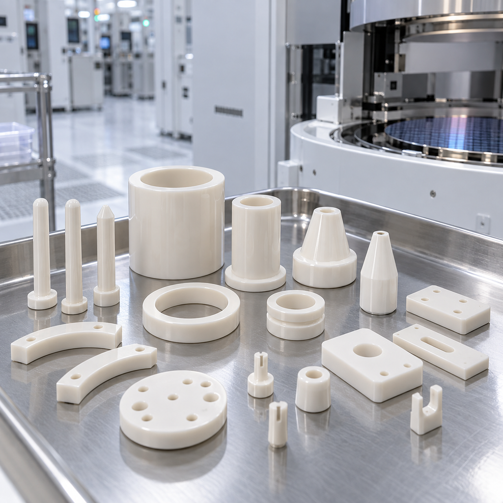
Structural ceramics play a critical role in semiconductor manufacturing equipment because many process components must operate under conditions that are difficult for conventional metals and polymers. Depending on the process, equipment parts may be exposed to: Advanced ceramics are used in wafer handling, lithography, etching, deposition, thermal processing, cleaning, inspection, back grinding and other semiconductor

Structural Ceramics for Semiconductor Manufacturing: Component and Material Selection قراءة المزيد »

Ceramic Wafer End Effector Design: Material, Weight, Flatness and Particle Control

A ceramic wafer end effector—also called a wafer handling blade, robot blade or wafer transfer arm—is the part of a semiconductor robot that directly supports and transfers wafers between process chambers, load ports, aligners, inspection stations and wafer carriers. Although its geometry may appear simple, the end effector directly affects wafer positioning accuracy, transfer speed,

Ceramic Wafer End Effector Design: Material, Weight, Flatness and Particle Control قراءة المزيد »

Wafer Chucking Force: Vacuum Pressure, Contact Area and Wafer Flatness

Wafer chucking force is one of the most important design parameters in semiconductor wafer handling, inspection, lithography, grinding, coating and precision machining equipment. A vacuum chuck must hold the wafer securely against acceleration, vibration and process loads. At the same time, it must avoid excessive local stress, backside contamination, wafer deformation and imprinting of the

Wafer Chucking Force: Vacuum Pressure, Contact Area and Wafer Flatness قراءة المزيد »

Ceramic Wafer Support Pins: Material Selection, Flatness and Particle Control

Ceramic wafer support pins are small but critical components in semiconductor processing equipment. They support, lift, position or temporarily separate wafers during transfer between a robot arm, process chamber, electrostatic chuck, vacuum chuck or wafer stage. Although their geometry is relatively simple, wafer support pins directly contact or approach sensitive wafer surfaces. Variations in pin

Ceramic Wafer Support Pins: Material Selection, Flatness and Particle Control قراءة المزيد »

Ceramic Vacuum Chuck Design: Porosity, Flatness and Wafer Holding Performance

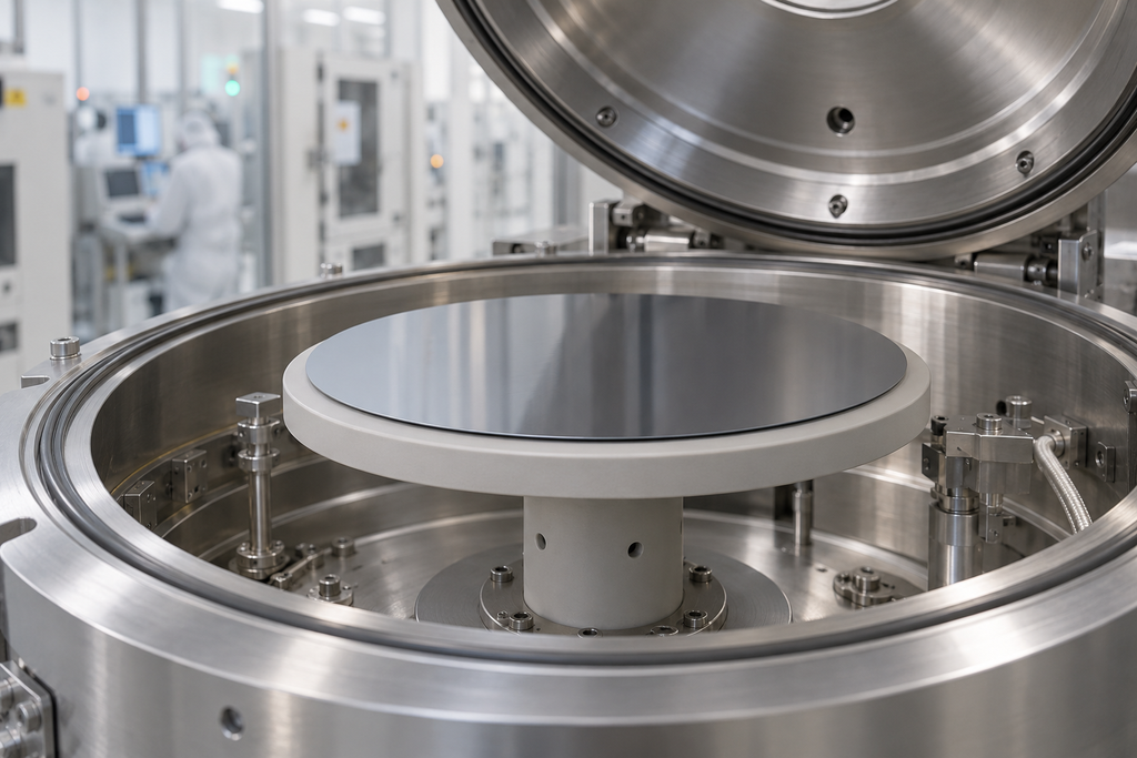
Vacuum chucks are essential components in modern semiconductor manufacturing. They securely hold silicon, silicon carbide (SiC), sapphire, glass, and compound semiconductor wafers during lithography, inspection, grinding, polishing, laser processing, metrology, and wafer bonding. Among various chuck technologies, porous ceramic vacuum chuck have become the preferred solution because they provide uniform vacuum distribution, excellent dimensional stability,

Ceramic Vacuum Chuck Design: Porosity, Flatness and Wafer Holding Performance قراءة المزيد »

Ceramic Components Failure Analysis: Cracks, Chipping, Wear and Thermal Damage

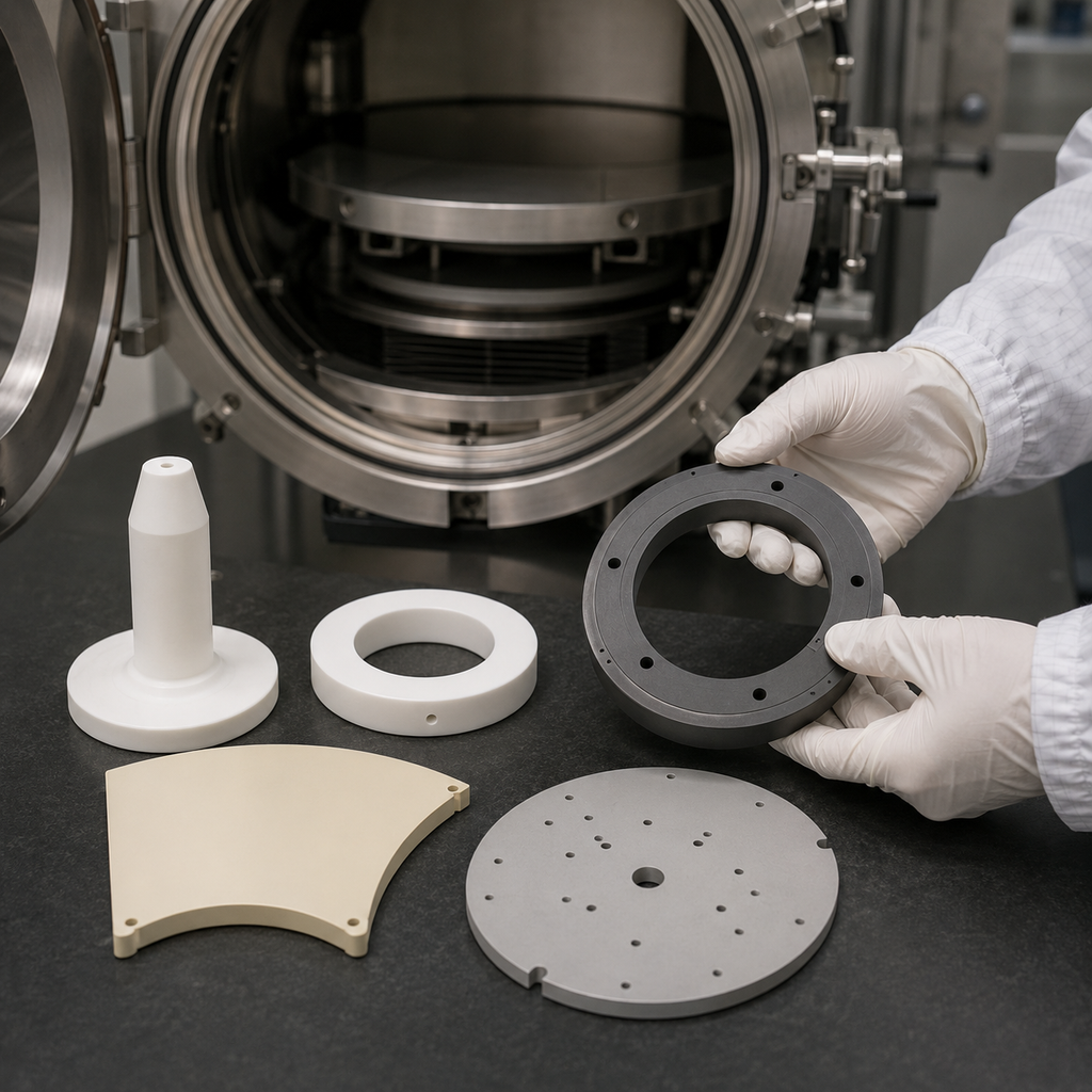
Advanced ceramic components are widely used in semiconductor equipment, vacuum systems, precision machinery, electrical insulation, chemical processing and high-temperature applications. Materials such as alumina, zirconia, aluminum nitride, silicon carbide and silicon nitride provide excellent hardness, wear resistance, corrosion resistance, electrical insulation and dimensional stability. Despite these advantages, ceramic components can still fail. Unlike most metals,

Ceramic Components Failure Analysis: Cracks, Chipping, Wear and Thermal Damage قراءة المزيد »

Alumina Ceramic Purity Levels Explained: 95%, 99%, 99.5% and 99.9% Compared

Alumina ceramic, also known as aluminum oxide ceramic or Al₂O₃ ceramic, is one of the most widely used technical ceramic materials. It offers a practical combination of electrical insulation, mechanical strength, hardness, wear resistance, thermal stability and corrosion resistance. However, not all alumina ceramics are the same. Commercial alumina materials are commonly identified by their

Alumina Ceramic Purity Levels Explained: 95%, 99%, 99.5% and 99.9% Compared قراءة المزيد »

Structural Ceramics for Semiconductor Manufacturing: Key Materials and Equipment Applications

Semiconductor manufacturing requires materials that can operate reliably under high temperature, plasma exposure, chemical corrosion, vacuum conditions and strict cleanliness requirements. In many process tools, metal and plastic components cannot meet these demanding conditions. This is why structural ceramics are widely used in semiconductor equipment. Structural ceramics are advanced ceramic materials designed to provide mechanical

Structural Ceramics for Semiconductor Manufacturing: Key Materials and Equipment Applications قراءة المزيد »

Semiconductor Wafer Boat Materials: SiC, Quartz and Alumina Compared

In semiconductor manufacturing, wafer boats are used to hold and support wafers during high-temperature processes such as diffusion, oxidation, annealing and LPCVD. Although the structure of a wafer boat may look simple, the material choice is very important. Different materials can affect thermal stability, contamination control, mechanical strength, service life and overall process reliability. Among

Semiconductor Wafer Boat Materials: SiC, Quartz and Alumina Compared قراءة المزيد »