Teollisuuden uutiset

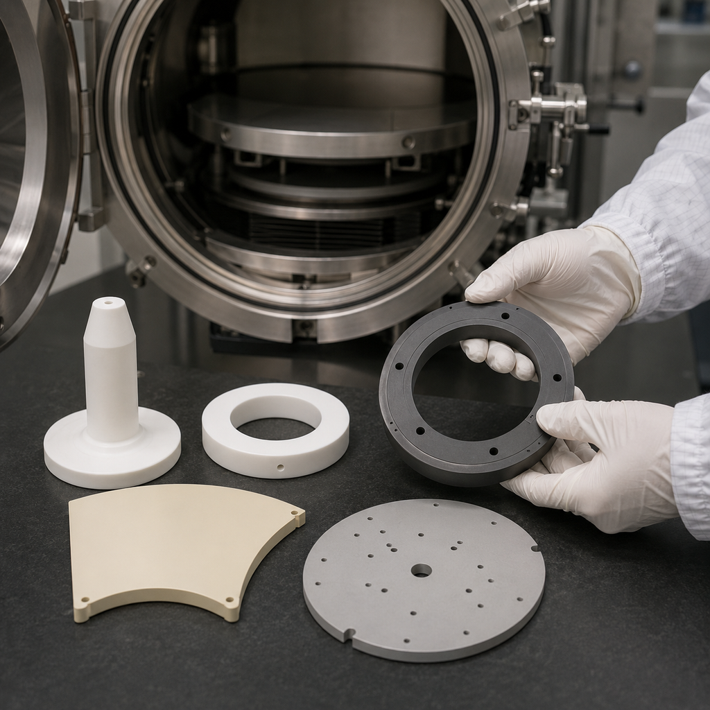
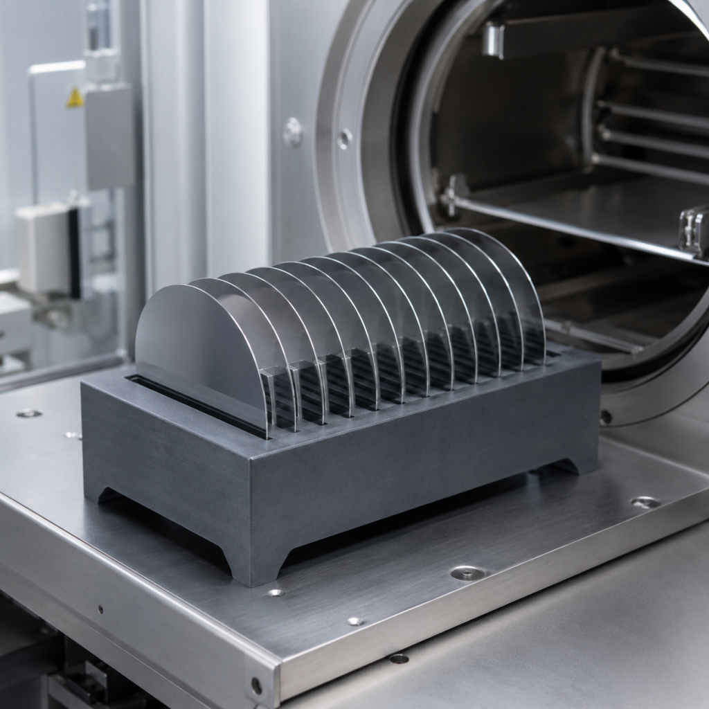
SiC Wafer Boats for 200mm and 300mm Semiconductor Furnaces: Slot Pitch, Purity, Thermal Shock, Particle Control and Cleaning Requirements

Silicon carbide wafer boats are critical furnace components used to support and position semiconductor wafers during high-temperature batch processes such as oxidation, annealing, diffusion and LPCVD. For 200mm and 300mm wafer processing, the wafer boat is much more than a simple ceramic carrier. Its slot geometry determines wafer positioning. Its dimensional stability influences process uniformity. […]
SiC Wafer Boats for 200mm and 300mm Semiconductor Furnaces: Slot Pitch, Purity, Thermal Shock, Particle Control and Cleaning Requirements Lue lisää »

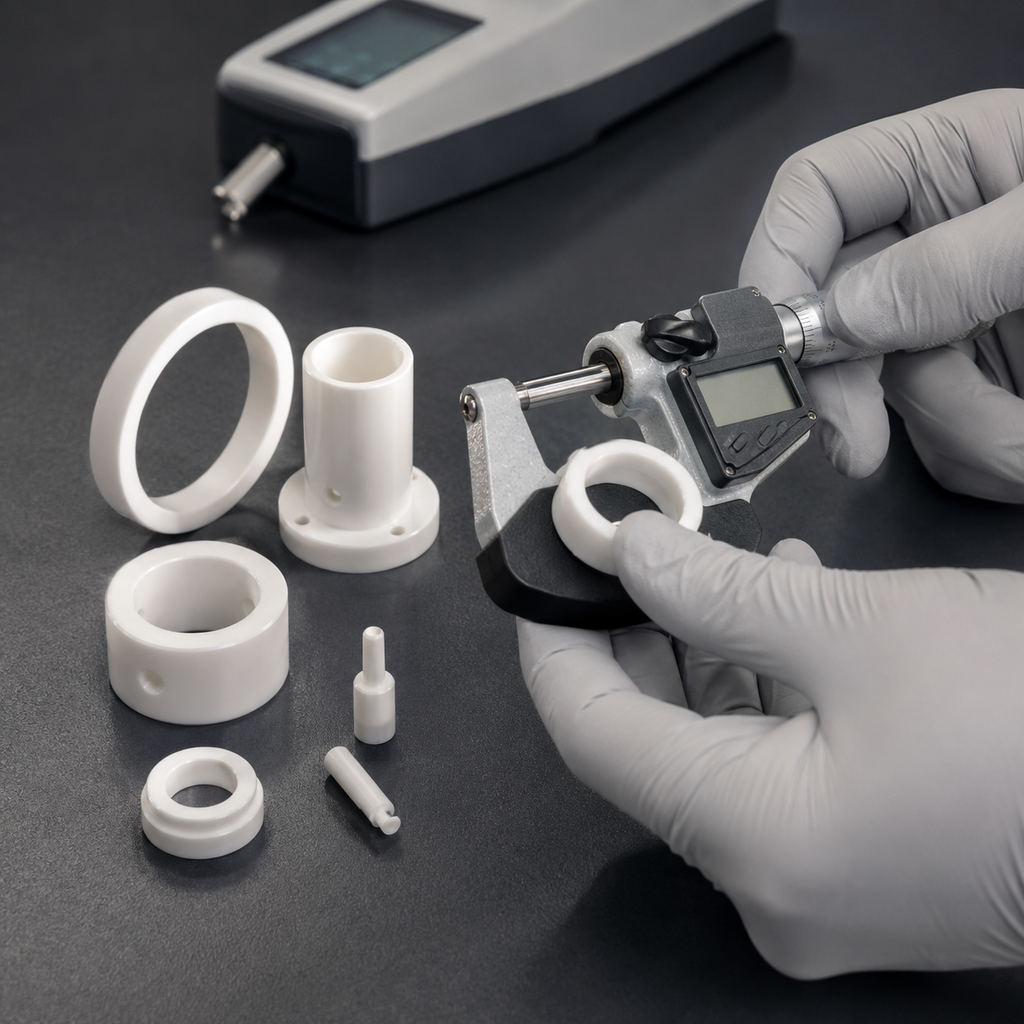
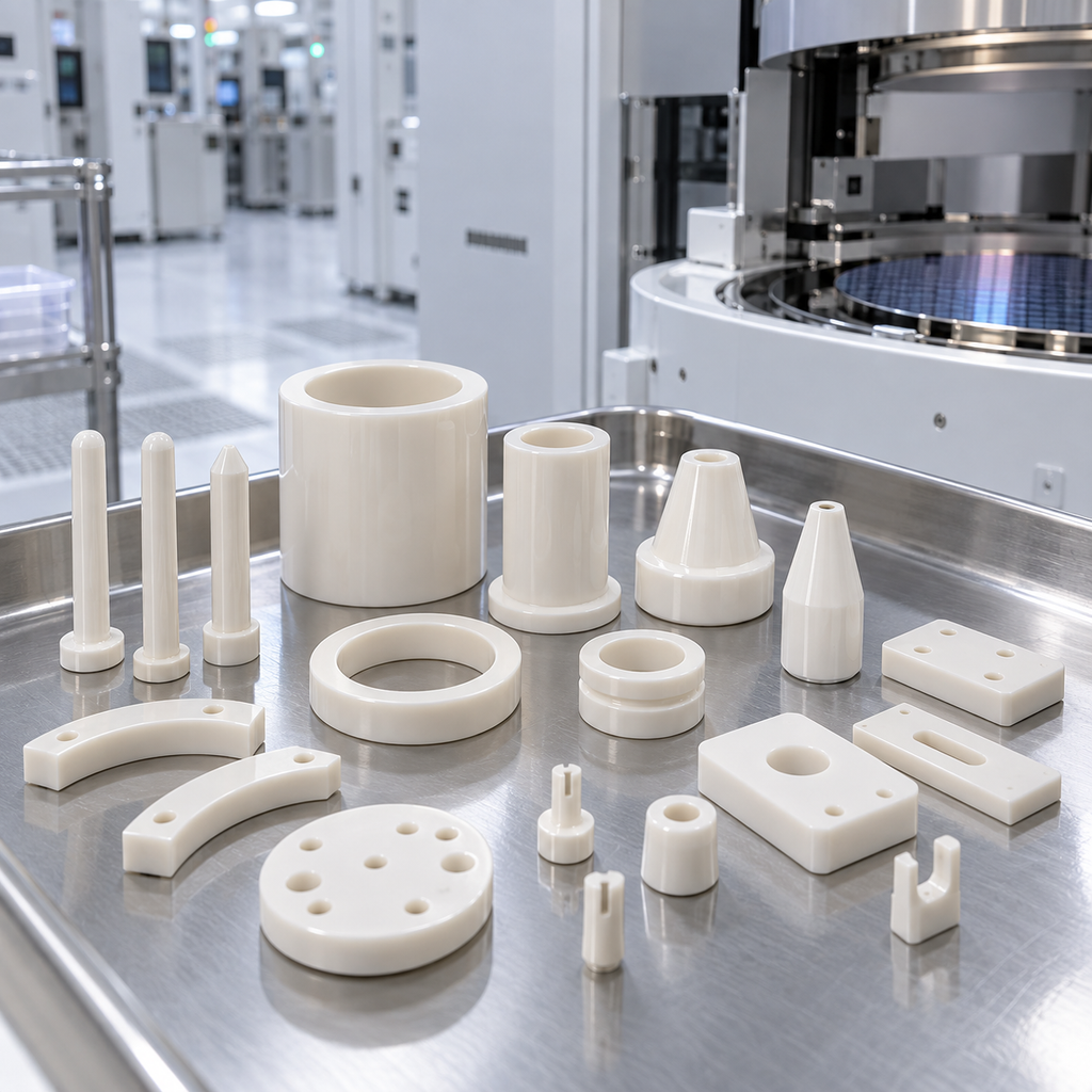
High-Purity Zirconia Ceramic Parts for Semiconductor Equipment: YSZ Purity, Wear Resistance, Surface Finish, Contamination Control and Custom Machining

Semiconductor equipment contains many small mechanical components that rarely attract the same attention as wafer chucks, heaters or process chambers, yet their material quality can directly influence equipment stability and contamination performance. Guide pins, positioning blocks, bushings, sleeves, nozzles, wear pads, insulating spacers, precision shafts and other contact components may operate for millions of cycles

High-Purity Zirconia Ceramic Parts for Semiconductor Equipment: YSZ Purity, Wear Resistance, Surface Finish, Contamination Control and Custom Machining Lue lisää »

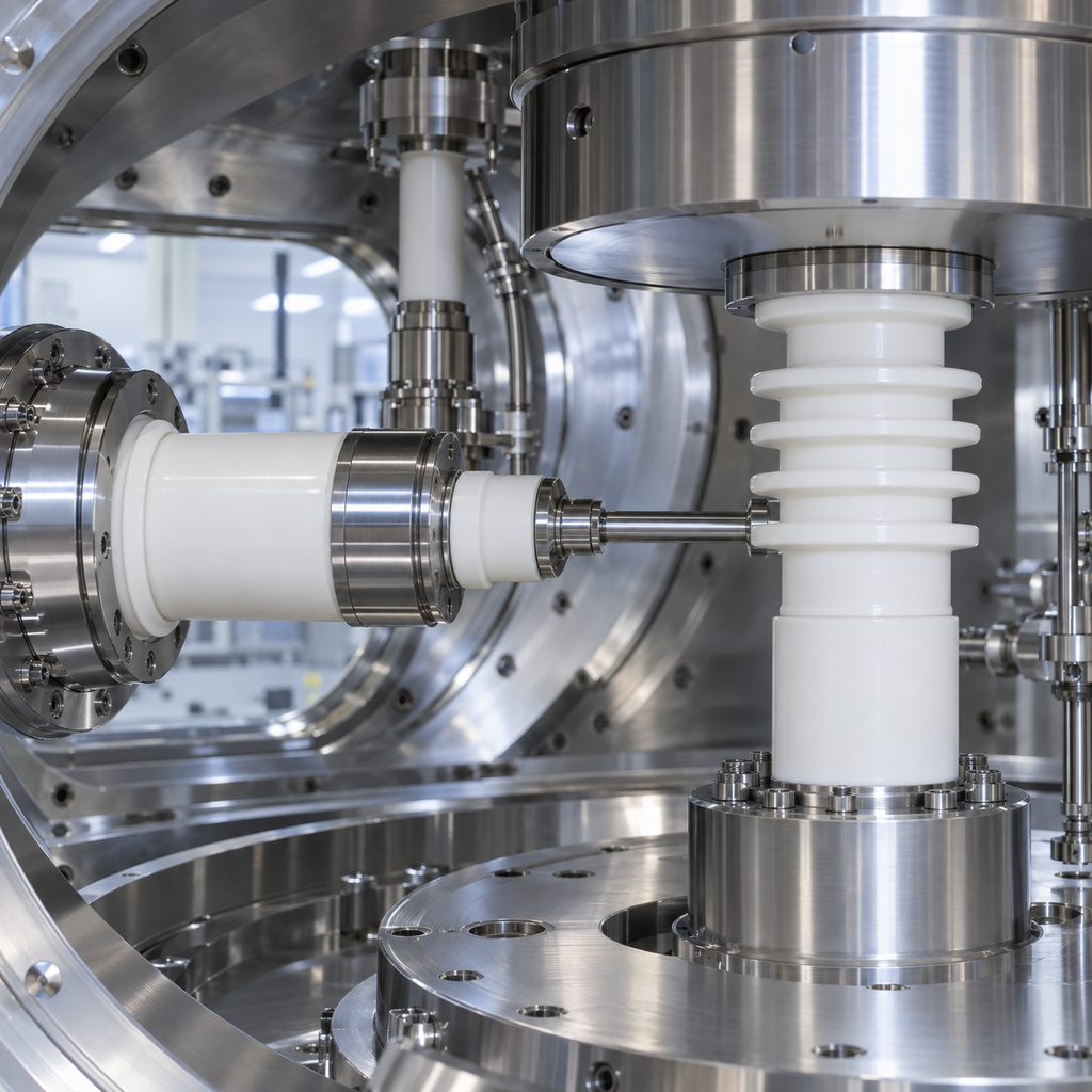
High-Voltage Alumina Ceramic Insulators for Ion Implantation Equipment: Dielectric Strength, Vacuum Outgassing, Surface Tracking and Thermal Shock

on implantation equipment uses accelerated ion beams to introduce controlled dopants into semiconductor wafers. Producing and transporting these beams requires high voltages, stable vacuum conditions and precise control of electrically isolated components. Within the ion source, extraction system, acceleration column and beamline, ceramic insulators separate energized electrodes from grounded structures. These components may appear simple,

High-Voltage Alumina Ceramic Insulators for Ion Implantation Equipment: Dielectric Strength, Vacuum Outgassing, Surface Tracking and Thermal Shock Lue lisää »

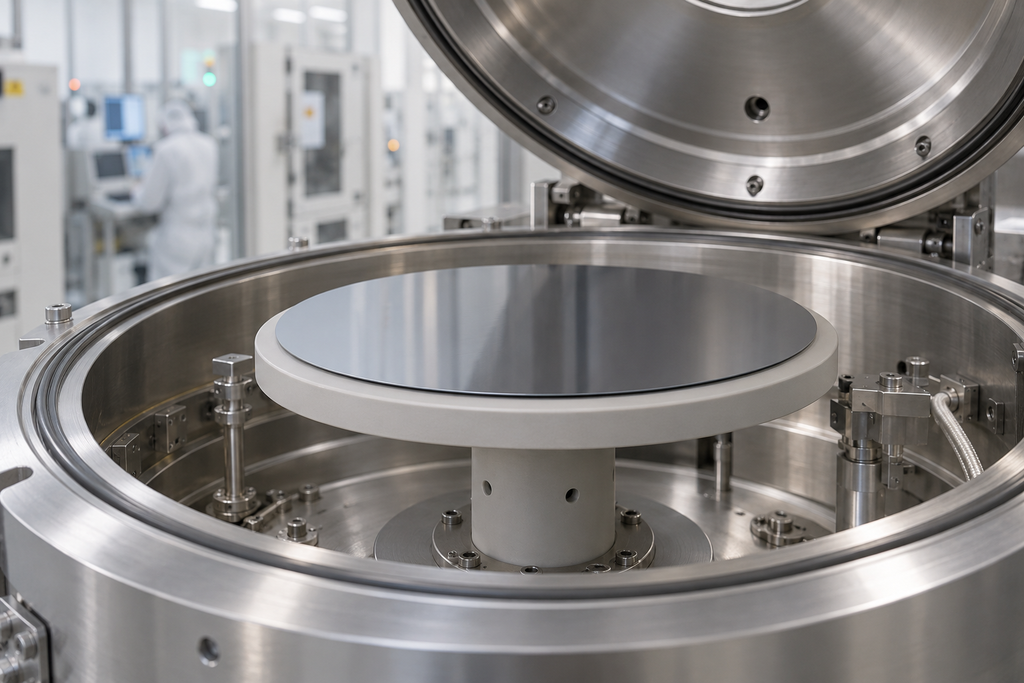
AlN Ceramic Heater Pedestals for 300mm ALD and CVD Equipment: Temperature Uniformity, Embedded Circuits, Flatness and Vacuum Reliability

As semiconductor devices move toward more complex three-dimensional structures, deposition processes must create increasingly uniform films across deep trenches, narrow gaps and large wafer surfaces. Atomic layer deposition (ALD) and chemical vapor deposition (CVD) therefore depend not only on precursor chemistry and chamber design, but also on precise wafer temperature control. For 300mm processing equipment,

AlN Ceramic Heater Pedestals for 300mm ALD and CVD Equipment: Temperature Uniformity, Embedded Circuits, Flatness and Vacuum Reliability Lue lisää »

Plasma-Resistant Ceramic Components for Semiconductor Etch Chambers: Al₂O₃, Y₂O₃, AlN and SiC Material Selection

Semiconductor plasma etch chambers expose internal components to fluorine-, chlorine-, bromine- and oxygen-containing gases, energetic ions, ultraviolet radiation, vacuum and repeated thermal cycling. Under these conditions, chamber hardware can gradually erode, change surface chemistry and release particles or metallic contaminants. Even a component that remains mechanically intact may become unsuitable if it alters process stability

Plasma-Resistant Ceramic Components for Semiconductor Etch Chambers: Al₂O₃, Y₂O₃, AlN and SiC Material Selection Lue lisää »

HBN Ceramic vs. hBN Single Crystal: Structure, Machinability, Thermal Performance and Semiconductor Applications

Hexagonal boron nitride appears in many semiconductor material catalogs, but the term “hBN” can describe products with very different structures and uses. A machinable hBN ceramic component, a device-grade hBN single crystal, a pyrolytic boron nitride crucible and an hBN powder may all have the same basic chemical composition—boron and nitrogen—yet they cannot be used

HBN Ceramic vs. hBN Single Crystal: Structure, Machinability, Thermal Performance and Semiconductor Applications Lue lisää »

High-Purity Zirconia Ceramic Parts Specification Guide: Y-TZP Composition, Density, Surface Finish and Machining Tolerances

High-purity zirconia ceramic parts are widely selected for precision equipment that requires high fracture toughness, wear resistance, electrical insulation and a smooth working surface. Typical components include ceramic bushings, positioning pins, valve parts, sleeves, guides, nozzles, sealing elements and precision fixtures. However, specifying a part simply as “zirconia ceramic” is not sufficient. Zirconia properties depend

High-Purity Zirconia Ceramic Parts Specification Guide: Y-TZP Composition, Density, Surface Finish and Machining Tolerances Lue lisää »

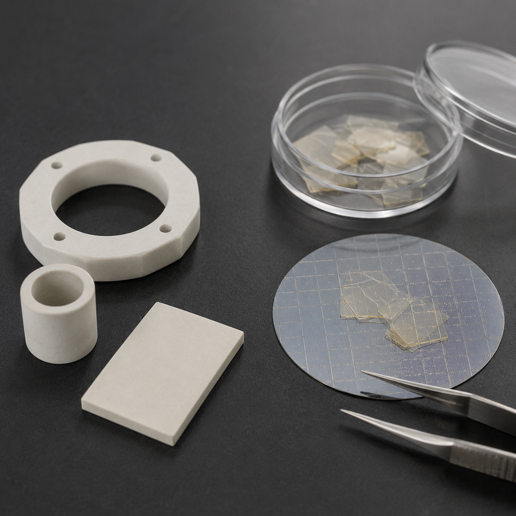
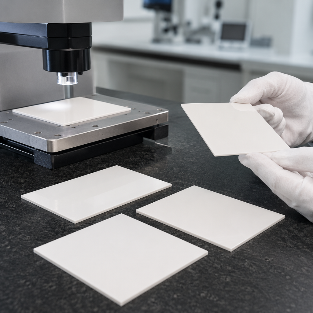
Polished Alumina Substrate Specification Guide: Purity, Flatness, Surface Roughness and Edge Quality

Polished alumina substrates are widely used in semiconductor equipment, power electronics, thin-film circuits, sensors, optoelectronics and precision industrial components. They provide electrical insulation, mechanical strength, dimensional stability and resistance to heat and chemicals. However, “polished alumina substrate” is not a complete purchasing specification. Two substrates with the same length, width and thickness may behave very

Polished Alumina Substrate Specification Guide: Purity, Flatness, Surface Roughness and Edge Quality Lue lisää »

SiC Wafer Boat Design Guide: Slot Pitch, Wafer Capacity, Thermal Uniformity and Particle Control

In semiconductor thermal processing, a wafer boat is more than a simple carrier. Its geometry influences wafer spacing, loading stability, gas flow, temperature distribution and particle performance throughout the process. Silicon carbide wafer boats are commonly considered for diffusion, oxidation, annealing, LPCVD and other high-temperature semiconductor processes because silicon carbide offers excellent thermal stability, mechanical

SiC Wafer Boat Design Guide: Slot Pitch, Wafer Capacity, Thermal Uniformity and Particle Control Lue lisää »

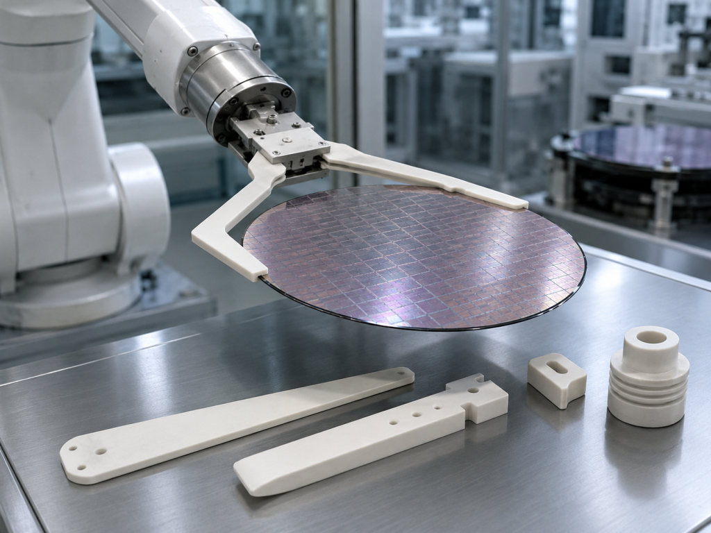
Ceramic End Effectors for Wafer Handling: Materials, ESD Control, Precision and Selection Guide

Wafer handling is one of the most delicate operations in semiconductor manufacturing. During transfer between load ports, process chambers, inspection stations and storage systems, wafers must be moved accurately without introducing particles, scratches, electrostatic damage or mechanical stress. The end effector, sometimes called a wafer handling blade, robot blade or wafer fork, is the component

Ceramic End Effectors for Wafer Handling: Materials, ESD Control, Precision and Selection Guide Lue lisää »

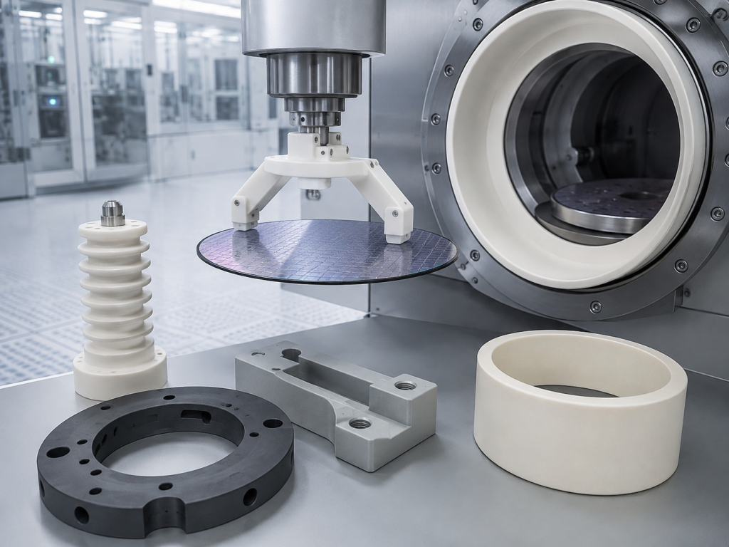
Structural Ceramics for Semiconductor Manufacturing: Materials, Properties and Key Applications

Semiconductor manufacturing equipment operates under some of the most demanding conditions found in modern industrial production. Components may be exposed to high temperatures, plasma, corrosive gases, vacuum environments, rapid thermal cycling, aggressive cleaning processes and extremely strict contamination requirements. Under these conditions, conventional metals and polymers are not always suitable. This is why structural ceramics

Structural Ceramics for Semiconductor Manufacturing: Materials, Properties and Key Applications Lue lisää »

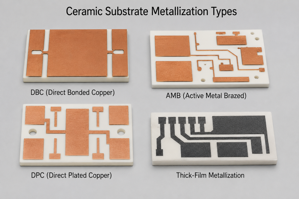
Ceramic Substrates Metallization Guide: DBC, AMB, DPC and Thick-Film Processes

Ceramic substrates are widely used in power electronics, semiconductor equipment, automotive electronics, LED modules, industrial lasers and other applications that require electrical insulation together with effective heat dissipation. However, selecting the ceramic material is only part of the design process. The method used to create the metal circuit on the ceramic surface can have an

Ceramic Substrates Metallization Guide: DBC, AMB, DPC and Thick-Film Processes Lue lisää »