xinkehui

Keraamiset substraatit: Puolijohteet: Ydinmateriaalivallankumous tekoälylaskennan, optisten moduulien ja tehopuolijohteiden voimanlähteinä

As artificial intelligence computing accelerates, data transmission speeds increase, and next-generation power electronics continue to evolve, semiconductor packaging technologies are undergoing a fundamental transformation. Conventional substrate materials are increasingly facing limitations in thermal management, electrical performance, and integration density. Against this backdrop, ceramic substrates are emerging from niche applications to become critical enabling materials for […]
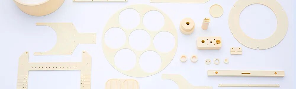
Keraamiset substraatit: Puolijohteet: Ydinmateriaalivallankumous tekoälylaskennan, optisten moduulien ja tehopuolijohteiden voimanlähteinä Read More »

Alumiinikeraamiset komponentit puolijohdelaitteissa: Alumiinioksidit: toiminnot, rakenteet ja kehittyneet sovellukset

As semiconductor devices continue evolving toward smaller nodes, higher integration density, and greater processing precision, the demand for ultra-clean, heat-resistant, and plasma-stable materials inside semiconductor equipment has increased significantly. Among advanced engineering ceramics, high-purity alumina ceramic (Al₂O₃) remains one of the most widely used materials across semiconductor manufacturing systems. From plasma etching chambers to wafer

Alumiinikeraamiset komponentit puolijohdelaitteissa: Alumiinioksidit: toiminnot, rakenteet ja kehittyneet sovellukset Read More »

Puolijohdelaitteiden tarkat keraamiset komponentit: Kattava katsaus kehittyneisiin keraamisiin sovelluksiin

As semiconductor manufacturing advances toward smaller process nodes, higher integration density, and ultra-clean production environments, precision ceramic components have become indispensable throughout semiconductor fabrication equipment. Advanced ceramics are widely used in lithography, etching, thin-film deposition, ion implantation, CMP, packaging, and wafer handling systems. These ceramic components serve critical functions including wafer support, plasma resistance, insulation,

Puolijohdelaitteiden tarkat keraamiset komponentit: Kattava katsaus kehittyneisiin keraamisiin sovelluksiin Read More »

Kehittyneet keraamiset materiaalit puolijohteiden valmistuksessa: Erittäin puhdas, äärimmäinen lämmönkestävyys ja erittäin kova suorituskyky.

As semiconductor technology continues to evolve toward smaller nodes, higher integration density, and more complex manufacturing processes, the demand for advanced materials inside semiconductor equipment has increased dramatically. Modern semiconductor fabrication environments require materials capable of withstanding extreme temperatures, corrosive plasma exposure, ultra-clean vacuum conditions, and high mechanical stress while maintaining dimensional stability and contamination

Kehittyneet keraamiset materiaalit puolijohteiden valmistuksessa: Erittäin puhdas, äärimmäinen lämmönkestävyys ja erittäin kova suorituskyky. Read More »

Kehittyneet keraamiset komponentit puolijohdevalmistuksessa: Sähköstaattisen kiinnittimen periaatteet ja suuntaukset: Sähköstaattisen kiinnittimen periaatteet ja suuntaukset

1. Introduction: Role of Advanced Ceramics in Semiconductor Equipment In modern semiconductor manufacturing, equipment operates under extreme conditions such as vacuum environments, high temperatures, plasma exposure, and ultra-precision motion control. Traditional metallic materials often fail to meet the combined requirements of stability, cleanliness, electrical insulation, and thermal management. Advanced engineering ceramics—such as alumina (Al₂O₃), aluminum

Kehittyneet keraamiset komponentit puolijohdevalmistuksessa: Sähköstaattisen kiinnittimen periaatteet ja suuntaukset: Sähköstaattisen kiinnittimen periaatteet ja suuntaukset Read More »

Piikarbidi (SiC) keramiikka puolijohdeteollisuudessa: Siilitehtaat: sovellukset, ominaisuudet ja tulevaisuuden näkymät

Silicon carbide (SiC) ceramics have become increasingly important in the semiconductor industry due to their exceptional thermal, mechanical, chemical, and electrical properties. Beyond their role as wide-bandgap semiconductor substrates for power devices, SiC ceramics are widely used in semiconductor manufacturing equipment, packaging, and thermal management systems. This article provides a scientific overview of SiC ceramics

Piikarbidi (SiC) keramiikka puolijohdeteollisuudessa: Siilitehtaat: sovellukset, ominaisuudet ja tulevaisuuden näkymät Read More »

Tarkkuuskeramiikka puolijohdelaitteissa: Ydinroolit ja teollisuuden kehityssuuntaukset

1. Introduction Precision ceramics refer to high-performance advanced ceramic components used in semiconductor manufacturing equipment. These components are typically designed with complex structures, ultra-high purity, and extremely tight dimensional tolerances. They play a critical role in ensuring the stability, accuracy, and reliability of semiconductor fabrication processes. With the rapid expansion of the global semiconductor industry

Tarkkuuskeramiikka puolijohdelaitteissa: Ydinroolit ja teollisuuden kehityssuuntaukset Read More »

Keraamiset komponentit puolijohdelaitteissa: Keraamiset keraamiset komponentit: sovellukset ja hyödyt

In semiconductor manufacturing, precision, purity, and thermal stability are critical requirements. As device geometries continue to shrink and process environments become more extreme, traditional metal components often fail to meet performance demands. This is where advanced ceramic materials play a crucial role. Ceramic components are widely used in semiconductor equipment due to their exceptional properties

Keraamiset komponentit puolijohdelaitteissa: Keraamiset keraamiset komponentit: sovellukset ja hyödyt Read More »