xinkehui

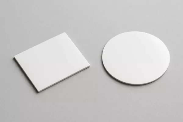
陶瓷基板:推動人工智慧運算、光學模組和功率半導體的核心材料革命

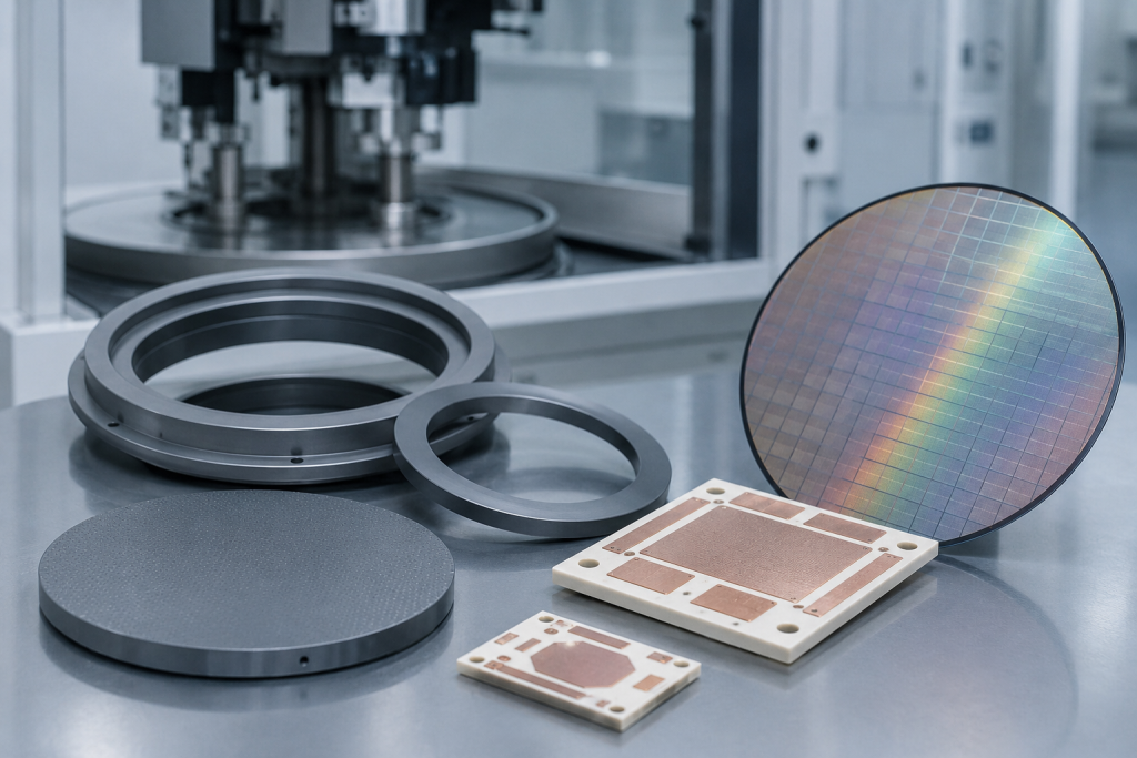
As artificial intelligence computing accelerates, data transmission speeds increase, and next-generation power electronics continue to evolve, semiconductor packaging technologies are undergoing a fundamental transformation. Conventional substrate materials are increasingly facing limitations in thermal management, electrical performance, and integration density. Against this backdrop, ceramic substrates are emerging from niche applications to become critical enabling materials for […]

陶瓷基板:推動人工智慧運算、光學模組和功率半導體的核心材料革命 閱讀更多 »
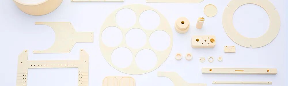
半導體設備中的氧化鋁陶瓷元件:功能、結構和先進應用

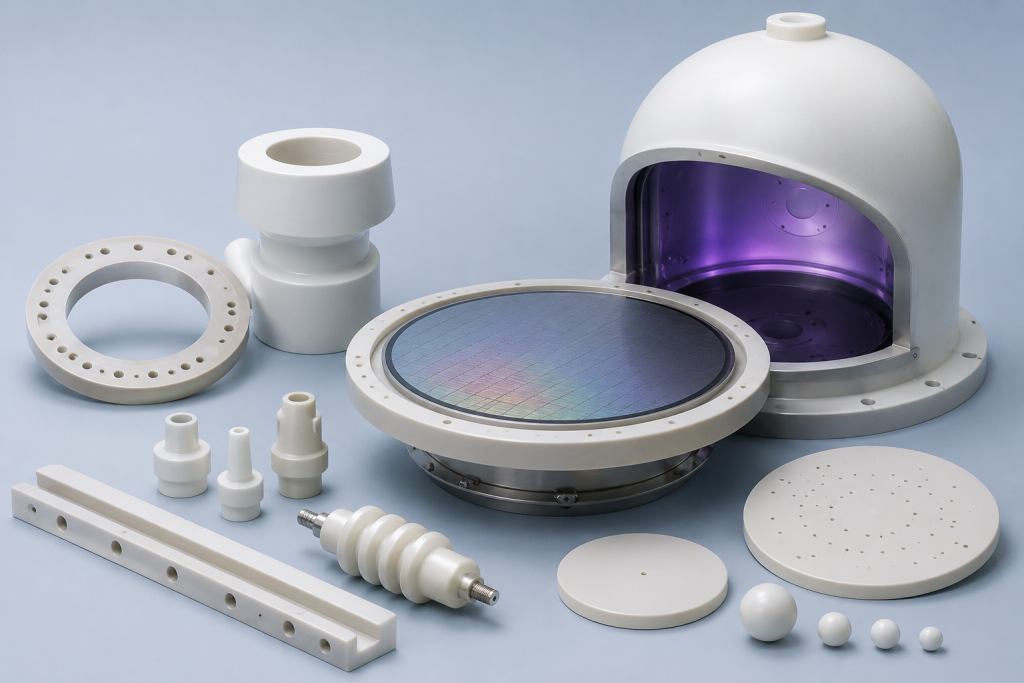
As semiconductor devices continue evolving toward smaller nodes, higher integration density, and greater processing precision, the demand for ultra-clean, heat-resistant, and plasma-stable materials inside semiconductor equipment has increased significantly. Among advanced engineering ceramics, high-purity alumina ceramic (Al₂O₃) remains one of the most widely used materials across semiconductor manufacturing systems. From plasma etching chambers to wafer

半導體設備中的氧化鋁陶瓷元件:功能、結構和先進應用 閱讀更多 »

半導體設備的精密陶瓷元件:先進陶瓷應用的全面概述

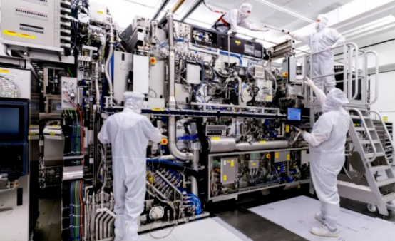
As semiconductor manufacturing advances toward smaller process nodes, higher integration density, and ultra-clean production environments, precision ceramic components have become indispensable throughout semiconductor fabrication equipment. Advanced ceramics are widely used in lithography, etching, thin-film deposition, ion implantation, CMP, packaging, and wafer handling systems. These ceramic components serve critical functions including wafer support, plasma resistance, insulation,

半導體設備的精密陶瓷元件:先進陶瓷應用的全面概述 閱讀更多 »

半導體製造中的先進陶瓷材料:高純度、極高耐熱性和超硬性能

As semiconductor technology continues to evolve toward smaller nodes, higher integration density, and more complex manufacturing processes, the demand for advanced materials inside semiconductor equipment has increased dramatically. Modern semiconductor fabrication environments require materials capable of withstanding extreme temperatures, corrosive plasma exposure, ultra-clean vacuum conditions, and high mechanical stress while maintaining dimensional stability and contamination

半導體製造中的先進陶瓷材料:高純度、極高耐熱性和超硬性能 閱讀更多 »

半導體製造中的先進陶瓷元件:靜電夾頭原理與趨勢

1. Introduction: Role of Advanced Ceramics in Semiconductor Equipment In modern semiconductor manufacturing, equipment operates under extreme conditions such as vacuum environments, high temperatures, plasma exposure, and ultra-precision motion control. Traditional metallic materials often fail to meet the combined requirements of stability, cleanliness, electrical insulation, and thermal management. Advanced engineering ceramics—such as alumina (Al₂O₃), aluminum

半導體製造中的先進陶瓷元件:靜電夾頭原理與趨勢 閱讀更多 »

半導體產業中的碳化矽 (SiC) 陶瓷:應用、特性與未來展望

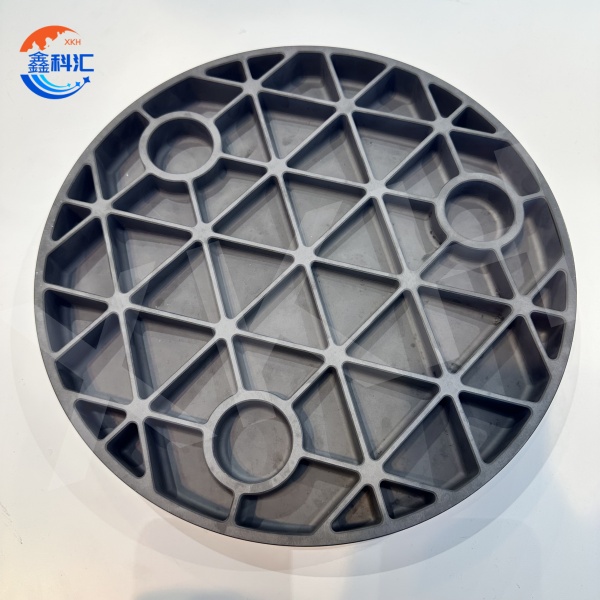
Silicon carbide (SiC) ceramics have become increasingly important in the semiconductor industry due to their exceptional thermal, mechanical, chemical, and electrical properties. Beyond their role as wide-bandgap semiconductor substrates for power devices, SiC ceramics are widely used in semiconductor manufacturing equipment, packaging, and thermal management systems. This article provides a scientific overview of SiC ceramics

半導體產業中的碳化矽 (SiC) 陶瓷:應用、特性與未來展望 閱讀更多 »

精密陶瓷在半導體設備中的應用:核心角色與產業發展趨勢

1. Introduction Precision ceramics refer to high-performance advanced ceramic components used in semiconductor manufacturing equipment. These components are typically designed with complex structures, ultra-high purity, and extremely tight dimensional tolerances. They play a critical role in ensuring the stability, accuracy, and reliability of semiconductor fabrication processes. With the rapid expansion of the global semiconductor industry

精密陶瓷在半導體設備中的應用:核心角色與產業發展趨勢 閱讀更多 »

半導體設備中的陶瓷元件:應用與優點

In semiconductor manufacturing, precision, purity, and thermal stability are critical requirements. As device geometries continue to shrink and process environments become more extreme, traditional metal components often fail to meet performance demands. This is where advanced ceramic materials play a crucial role. Ceramic components are widely used in semiconductor equipment due to their exceptional properties

半導體設備中的陶瓷元件:應用與優點 閱讀更多 »