
Wafer handling is one of the most delicate operations in semiconductor manufacturing. During transfer between load ports, process chambers, inspection stations and storage systems, wafers must be moved accurately without introducing particles, scratches, electrostatic damage or mechanical stress.
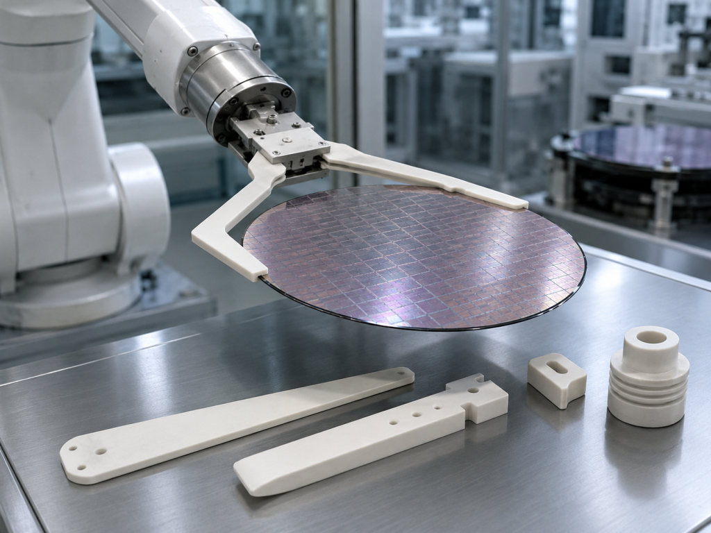
的 end effector, sometimes called a wafer handling blade, robot blade or wafer fork, is the component that directly supports or contacts the wafer during robotic transfer.
Because it operates close to highly sensitive wafer surfaces, the choice of end effector material has a direct influence on:
- 粒子產生
- Wafer cleanliness
- Electrostatic discharge risk
- 定位精度
- Mechanical stability
- 熱阻
- Equipment uptime
For these reasons, advanced technical ceramics are increasingly used for precision wafer handling components.
This guide explains the main ceramic materials used for wafer end effectors, their electrical and mechanical properties, ESD control methods, machining requirements and key considerations when selecting a custom ceramic end effector.
What Is a Wafer End Effector?
A wafer end effector is the part mounted at the end of a semiconductor robot arm that directly supports, carries or grips a wafer.
It is commonly used in:
- 晶圓搬運機器人
- Load lock systems
- 製程室
- PVD and CVD equipment
- 蝕刻系統
- Cleaning equipment
- Inspection systems
- Metrology equipment
- Automated material handling systems
Depending on the equipment design, the end effector may contact the wafer from below, hold it through edge contact or use vacuum-assisted handling.
Typical designs include:
- Fork-type end effectors
- Blade-type end effectors
- Paddle-type end effectors
- Vacuum end effectors
- Edge-grip end effectors
- Customized robotic wafer handling tools
Each configuration requires different mechanical, electrical and surface characteristics.
Why Use Ceramic End Effectors?
Traditional wafer handling components may be manufactured from metals or engineering polymers.
However, semiconductor processes increasingly require materials with higher cleanliness, dimensional stability and resistance to aggressive environments.
Ceramic end effectors can provide several important advantages.
Low Particle Generation
Particles generated during wafer transfer can cause defects during later processing steps.
Possible particle sources include:
- 機械磨損
- 表面磨損
- Material flaking
- Contact between wafer and handling components
- Edge damage
- Contamination from moving parts
High-quality technical ceramics offer excellent hardness and wear resistance, helping reduce surface degradation during repeated handling cycles.
Properly polished ceramic surfaces can also minimize friction between the end effector and the wafer.
Excellent Dimensional Stability
Robot positioning accuracy may depend on dimensional tolerances measured in micrometers.
If the end effector bends, twists or changes dimensions during operation, wafer positioning accuracy may decrease.
Ceramic materials generally provide:
- 高剛性
- Low deformation
- 良好的尺寸穩定性
- Excellent repeatability
This makes them suitable for precision wafer transfer systems.
High Temperature Capability
Some wafer handling operations take place near heated process chambers.
End effectors may therefore experience elevated temperatures or repeated thermal cycling.
Technical ceramics can maintain mechanical stability at temperatures where many polymers would lose strength or deform.
材料,例如:
- 氧化鋁
- 碳化矽
- 氮化鋁
- 氮化矽
can be selected depending on the operating temperature and thermal requirements.
Electrical Insulation or Controlled Conductivity
Electrical behavior is another important consideration.
Some applications require electrically insulating end effectors, while others require controlled electrical conductivity to reduce electrostatic charge accumulation.
This makes material selection especially important for ESD-sensitive semiconductor processes.
Common Materials for Ceramic Wafer End Effectors
Different ceramic materials provide different combinations of stiffness, electrical properties, wear resistance, thermal conductivity and cost.
Alumina Ceramic End Effectors
Alumina ceramic (Al₂O₃) is one of the most widely used materials for wafer handling components.
Common purity grades include:
- 95% alumina
- 96% alumina
- 99% alumina
- 99.5% alumina
- 99.7% or higher-purity alumina
For semiconductor applications, higher-purity materials are often preferred to reduce contamination risk.
主要優勢
Alumina provides:
- 高硬度
- 優異的耐磨性
- 良好的機械強度
- 高電阻率
- 良好的尺寸穩定性
- 良好的耐化學性
- Relatively cost-effective manufacturing
典型應用
Alumina wafer handling parts may be used in:
- Standard wafer transfer robots
- Inspection systems
- Load ports
- 真空設備
- Semiconductor automation systems
It is often a good general-purpose material when high electrical insulation is required.
ESD-Safe Ceramic End Effectors
For some semiconductor devices, excessive static charge can damage sensitive structures.
A conventional highly insulating ceramic surface may allow charge to accumulate.
To address this issue, ESD-safe ceramics can be engineered with controlled electrical resistivity.
Instead of behaving as a perfect electrical insulator, the material allows charge to dissipate gradually.
This reduces the risk of sudden electrostatic discharge.
Typical ESD-safe ceramics may use:
- Conductive ceramic additives
- Modified alumina compositions
- Composite ceramic materials
- Specialized surface treatments
The target resistivity depends on the equipment design and process requirements.
Why ESD Control Matters in Wafer Handling
Electrostatic charge can develop during wafer handling due to:
- Contact and separation between surfaces
- Robot movement
- 摩擦
- Dry cleanroom environments
- Polymer components
- Insulating surfaces
If charge accumulates and suddenly discharges, it may damage sensitive semiconductor structures.
Potential effects include:
- Device damage
- Electrical failure
- Latent defects
- Reduced production yield
For this reason, ESD control may be required for wafer handling equipment used in advanced semiconductor manufacturing.
Electrical Resistivity Requirements
When selecting an ESD-controlled ceramic end effector, the electrical resistivity should be specified carefully.
A material that is too insulating may not dissipate charge effectively.
A material that is too conductive may introduce other electrical risks.
The exact resistance range depends on:
- Semiconductor device sensitivity
- Robot grounding design
- Process environment
- Wafer type
- Equipment electrical architecture
Therefore, ESD performance should be evaluated as part of the complete wafer handling system rather than as an isolated material property.
Silicon Carbide End Effectors
碳化矽 (SiC) is suitable for demanding wafer handling applications requiring high stiffness, thermal stability and wear resistance.
主要優勢
SiC 提供:
- 高彈性模數
- 極佳的硬度
- 高導熱性
- 低熱膨脹
- 優異的耐磨性
- 高溫能力
- 良好的耐化學性
Because of its high stiffness-to-weight performance, SiC can be particularly useful for thin and long end effector structures.
典型應用
SiC end effectors may be used in:
- High-temperature wafer handling
- Precision transfer robots
- Vacuum systems
- Semiconductor process equipment
- High-speed automation
Specific SiC grades may also provide different electrical conductivity characteristics.
Silicon Nitride End Effectors
Silicon nitride is another advanced material suitable for precision robotic components.
Its advantages include:
- 高斷裂韌性
- 低密度
- High strength
- 良好的抗熱震性
- 優異的耐磨性
The relatively low density can help reduce the moving mass of robotic systems.
This can be beneficial in high-speed wafer transfer applications where acceleration and positioning repeatability are important.
Zirconia Ceramic End Effectors
Zirconia offers higher fracture toughness than many conventional technical ceramics.
It may be useful for smaller components or designs exposed to mechanical stress.
主要特性包括
- 高韌性
- 優異的耐磨性
- 高機械強度
- Good precision machining capability
- Smooth polished surfaces
However, zirconia has higher density and lower thermal conductivity than some other technical ceramics, so its suitability depends on the application.
Material Comparison
| 材質 | 關鍵優勢 | Electrical Property | Typical Application |
|---|---|---|---|
| 氧化鋁 | 性價比平衡 | Highly insulating | 一般晶圓處理 |
| ESD-Safe Alumina | Controlled charge dissipation | Controlled resistivity | ESD-sensitive devices |
| 碳化矽 | High stiffness and thermal stability | Grade dependent | High-precision, high-temperature handling |
| 氮化矽 | High strength with low density | Usually insulating | High-speed robotic handling |
| 氧化鋯 | 高斷裂韌性 | Insulating | Small precision mechanical components |
Precision Requirements for Wafer End Effectors
Material selection is only one part of the design.
End effectors also require extremely accurate machining.
Important specifications can include:
- 總長度
- Blade thickness
- Width
- 並行性
- 平整度
- Hole position
- Mounting interface
- Tip geometry
- 晶圓接觸位置
Because the end effector becomes part of the robot positioning system, dimensional errors may affect wafer centering and repeatability.
平整度
Flatness is particularly important for long and thin ceramic blades.
If the end effector is warped, the wafer may not sit correctly.
可能的後果包括:
- Unstable wafer support
- Positioning errors
- Uneven wafer contact
- Wafer slipping
- 機械應力
Flatness requirements should therefore be specified according to the wafer size and robot design.
並行性
Parallelism between the wafer support surface and the mounting surface affects robot calibration.
Poor parallelism may cause the wafer to tilt during handling.
This can become especially critical for:
- 200 mm wafers
- 300 mm wafers
- Thin wafers
- Advanced packaging substrates
表面粗糙度
The contact area between the wafer and ceramic end effector should be carefully finished.
Surface roughness can influence:
- 摩擦
- 粒子產生
- 晶圓刮傷
- Contact stability
Depending on the application, surfaces may be:
- Precision ground
- Lapped
- Fine polished
Extremely smooth surfaces are not always required across the entire component.
Usually, only the wafer contact zones and critical reference surfaces need the tightest finish.
Edge Finishing
Ceramic materials are hard but relatively brittle.
Sharp corners can become stress concentration points and may chip during handling.
Proper edge finishing may include:
- 倒角
- Radius edges
- Edge polishing
- Controlled deburring
This reduces the risk of ceramic particles being generated during equipment operation.
Lightweight Design
Robot performance depends partly on the mass of the moving components.
Reducing end effector weight can help improve:
- Acceleration
- Cycle time
- Positioning control
- Robot service life
However, lightweighting must not compromise rigidity.
Common design strategies include:
- Reducing unnecessary material
- Using thin-wall structures
- Adding pockets
- Optimizing cross sections
Ceramic stiffness allows relatively thin structures to remain mechanically stable when properly designed.
Wafer Contact Design
The wafer support area should be minimized while maintaining sufficient stability.
Reducing contact area can help reduce:
- Particle transfer
- 表面污染
- 摩擦
- Contact marks
Common contact designs include:
- Raised contact pads
- Point contacts
- Edge-support structures
- Narrow support rails
The correct geometry depends on the wafer thickness, robot acceleration and handling orientation.
真空末端效應器
Some ceramic end effectors use vacuum channels to hold wafers.
These parts may contain:
- Internal channels
- Vacuum ports
- Micro holes
- Grooves
- Sealing surfaces
Manufacturing these structures in ceramic requires precise machining.
Vacuum performance can be affected by:
- Surface flatness
- Hole position
- Channel geometry
- Seal quality
For these components, leak testing may also be required.
Wafer Size Considerations
The end effector should be designed specifically for the wafer diameter.
Common semiconductor wafer sizes include:
- 100 mm
- 150 mm
- 200 mm
- 300 mm
Larger wafers generally require:
- Higher stiffness
- Longer blade geometry
- Better flatness
- More precise robot calibration
Thin wafers introduce additional challenges because they can bend more easily.
Thin-Wafer Handling
Advanced packaging and power semiconductor manufacturing increasingly use thin wafers.
Thin wafers can be more sensitive to:
- Bending
- 龜裂
- Edge damage
- Local stress
End effector design should therefore distribute mechanical support carefully.
For thin-wafer applications, suppliers may need to evaluate:
- Contact point location
- Blade stiffness
- Acceleration
- Vacuum force
- Wafer sag
Cleanliness Requirements
Ceramic end effectors used in semiconductor equipment should be cleaned carefully before delivery.
Possible contamination sources include:
- Grinding residue
- Polishing compounds
- Metal particles from machining equipment
- Packaging contamination
Depending on the application, cleaning procedures may include:
- Ultrasonic cleaning
- DI water cleaning
- Chemical cleaning
- Cleanroom drying
- Clean packaging
Packaging should also prevent ceramic components from rubbing against each other during transportation.
Inspection Requirements
A precision wafer end effector may require inspection for:
- Dimensions
- 平整度
- 並行性
- 表面粗糙度
- Hole position
- Visual defects
- 邊緣崩角
- 材料純度
- Electrical resistivity
Typical inspection equipment may include:
- 坐標測量機
- 光學測量系統
- Surface profilometers
- Resistance meters
- Microscopes
Critical dimensions should be clearly marked on the engineering drawing.
Common Causes of End Effector Failure
Ceramic wafer handling components may fail because of:
Mechanical Impact
Unexpected collisions during robot movement can cause ceramic cracking.
Edge Chipping
Improper machining or assembly may create weak edges.
Excessive Mechanical Stress
Incorrect mounting or over-tightened fasteners may introduce stress.
熱衝擊
Rapid temperature changes may damage unsuitable ceramic materials.
Surface Wear
Repeated wafer contact can gradually change surface condition.
污染
Improper cleaning may introduce particles into the process environment.
Correct material selection and proper mechanical design can significantly reduce these risks.
How to Select a Ceramic End Effector
When selecting a ceramic wafer handling component, engineers should consider the complete operating environment.
Important questions include:
- What wafer size will be handled?
- What is the wafer thickness?
- What is the maximum operating temperature?
- Is ESD control required?
- Does the end effector operate in vacuum?
- Are corrosive gases present?
- What flatness and parallelism are required?
- What surface roughness is required?
- Is vacuum holding required?
- What robot mounting interface is used?
Providing this information allows the ceramic manufacturer to recommend the appropriate material and machining method.
RFQ Checklist for Custom Ceramic End Effectors
When requesting a quotation, buyers should provide:
- 2D or 3D engineering drawings
- Ceramic material
- 材料純度
- 晶圓直徑
- 整體尺寸
- Dimensional tolerances
- 平整度
- 並行性
- 表面粗糙度
- Electrical resistivity requirement
- 操作溫度
- 真空要求
- 數量
- Cleaning requirements
- Packaging requirements
If the material has not yet been selected, the operating environment should be provided so that the supplier can suggest a suitable ceramic.
Custom Ceramic End Effectors for Semiconductor Equipment
Modern semiconductor automation increasingly requires customized wafer handling components.
Typical customized features can include:
- Long thin ceramic blades
- Multi-point wafer support
- Vacuum channels
- Precision slots
- ESD-safe materials
- Special mounting interfaces
- Low-particle polished surfaces
- Complex CNC-machined structures
Manufacturability should ideally be considered during the design stage.
Extremely thin walls, sharp internal corners and unnecessary ultra-tight tolerances may increase machining difficulty and production cost.
Early cooperation between the equipment manufacturer and ceramic supplier can improve both performance and manufacturability.
總結
Ceramic end effectors are critical precision components in semiconductor wafer handling systems.
Their performance depends not only on the ceramic material, but also on:
- 電學特性
- Surface quality
- 平整度
- Dimensional accuracy
- Mechanical stiffness
- Wafer contact design
- 整潔
氧化鋁 provides excellent electrical insulation and general-purpose performance.
ESD-safe ceramics help control electrostatic charge in sensitive semiconductor processes.
碳化矽 offers high stiffness, wear resistance and thermal stability.
氮化矽 combines low density with high mechanical strength, while zirconia provides excellent toughness for precision mechanical components.
For custom wafer handling applications, the best results are achieved by evaluating the ceramic material, robot design, wafer dimensions, ESD requirements and process environment together.
XKH Ceramics provides customized technical ceramic components for semiconductor equipment, including precision wafer handling parts and ceramic end effectors. Customers can provide drawings, wafer size, material requirements, tolerances and operating conditions for technical evaluation and quotation.

