
Modern semiconductor manufacturing requires unprecedented levels of precision, cleanliness, thermal stability, and reliability. As chip architectures continue to evolve toward smaller nodes, higher power density, and advanced packaging technologies, conventional metallic materials increasingly face limitations in process environments involving plasma exposure, ultra-high vacuum, aggressive chemicals, and extreme temperatures.
Structural ceramics have therefore become indispensable materials in semiconductor equipment. Their unique combination of mechanical strength, wear resistance, thermal stability, corrosion resistance, and electrical properties makes them essential for wafer processing, handling, deposition, etching, and inspection systems.
This article provides an in-depth analysis of structural ceramics used in semiconductor manufacturing, including material types, critical properties, equipment applications, selection criteria, and future industry trends.
What Are Structural Ceramics?
Structural ceramics are engineered ceramic materials primarily designed for mechanical and functional performance under demanding operating conditions. Unlike decorative or traditional ceramics, advanced structural ceramics possess highly controlled microstructures and exceptional material properties.
In semiconductor environments, structural ceramics are expected to provide:
- High dimensional accuracy
- Độ ổn định nhiệt tuyệt vời
- Khả năng chống mài mòn do plasma
- Sản sinh ít hạt bụi
- Chemical inertness
- Độ tinh khiết cao
- Electrical insulation or conductivity depending on application
- Long-term reliability under vacuum conditions
As semiconductor processes become increasingly sensitive to contamination, even microscopic material degradation can affect wafer yield.
Why Structural Ceramics Matter in Semiconductor Manufacturing
Semiconductor equipment operates under conditions far more severe than conventional industrial systems.
Typical environments include:
Extreme temperature cycles
- Rapid heating and cooling
- Temperatures from cryogenic conditions to over 1600°C
- Thermal shock stress
Aggressive chemical exposure
- Axit
- Chất kiềm
- Reactive gases
- Cleaning chemistries
Plasma processing
Etching and deposition chambers use energetic plasmas capable of damaging conventional materials.
Ultra-clean environments
Particles measured in nanometers may significantly impact device performance.
Vacuum operation
Many semiconductor systems operate in:
- High vacuum
- Ultra-high vacuum
- Controlled atmosphere environments
Structural ceramics outperform metals in many of these situations because they resist corrosion, deformation, oxidation, and contamination.
Major Structural Ceramic Materials Used in Semiconductor Equipment
Different ceramic materials are selected according to process requirements.
Cacbua silic (SiC)
Silicon carbide is among the most important semiconductor structural ceramics.
Key properties:
- Độ cứng cực cao
- Độ dẫn nhiệt cao
- Khả năng chống mài mòn tuyệt vời
- Điện trở plasma
- Độ ổn định ở nhiệt độ cao
- Hệ số giãn nở nhiệt thấp
Ứng dụng:
- Khay đựng wafer
- Bộ kẹp chân không
- susceptors
- process trays
- robot arms
- wafer support structures
Reaction-bonded SiC and recrystallized SiC are commonly used in thermal processing systems.
Ưu điểm:
- Độ ổn định kích thước tuyệt vời
- Giảm ô nhiễm do hạt bụi
- Tuổi thọ cao
Alumina (Al₂O₃)
Alumina remains one of the most widely used ceramic materials due to cost-performance balance.
Typical properties:
- Cách điện
- Độ cứng cao
- Khả năng chống ăn mòn tốt
- Chi phí thấp
- Có sẵn sản phẩm có độ tinh khiết cao
Ứng dụng:
- Cách điện gốm
- nozzles
- guide components
- chamber parts
- positioning components
Purity levels often exceed:
99.5%
Ultra-high purity grades may exceed:
99.9%
Higher purity reduces contamination risk.
Zirconia (ZrO₂)
Zirconia provides exceptional fracture toughness.
Đặc điểm:
- Độ bền uốn cao
- Khả năng chống mài mòn
- Độ dẫn nhiệt thấp
- Excellent crack resistance
Ứng dụng:
- precision wear components
- bearings
- valve parts
- positioning systems
Transformation toughening mechanisms provide improved resistance to mechanical failure.
Nitrua nhôm (AlN)
Aluminum nitride is increasingly important because of its thermal conductivity.
Properties:
- Độ dẫn nhiệt cao
- Cách điện
- thermal expansion close to silicon
Ứng dụng:
- electrostatic chuck substrates
- thermal management components
- semiconductor heaters
AlN combines heat transfer capability with electrical isolation.
Quartz and Fused Silica
Although technically different from engineering structural ceramics, these materials remain essential.
Các ứng dụng bao gồm:
- process tubes
- thuyền bánh wafer
- diffusion equipment
- optical components
Ưu điểm:
- high purity
- hệ số giãn nở nhiệt thấp
- transparency
Key Applications of Structural Ceramics in Semiconductor Equipment
Structural ceramics appear throughout semiconductor production lines.
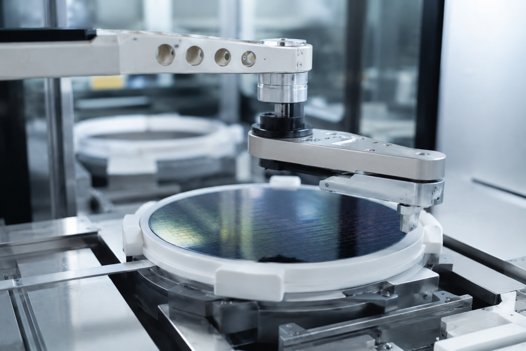
Hệ thống xử lý tấm wafer
Wafer transport systems require:
- dimensional precision
- low particle generation
- khả năng chống mài mòn
Components:
- robotic end effectors
- vacuum arms
- guide rails
- support pins
Ceramics reduce abrasion and contamination.
Electrostatic Chucks
Electrostatic chucks secure wafers during processing.
Requirements:
- controlled electrical properties
- thermal uniformity
- plasma resistance
Common materials:
- AlN
- SiC
- alumina composites
Performance directly influences process uniformity.
Các bộ phận của thiết bị khắc
Plasma etching chambers expose materials to energetic ions and reactive species.
Ceramic components include:
- vòng lấy nét
- bảng phân phối khí
- lớp lót buồng
- edge rings
SiC and high-purity alumina dominate these applications.
CVD and Epitaxy Systems
Chemical vapor deposition processes involve elevated temperatures.
Ceramic applications:
- susceptors
- process trays
- wafer carriers
- thermal shields
Thermal stability becomes critical.
CMP Systems
Chemical mechanical polishing requires components resistant to both chemistry and abrasion.
Ứng dụng:
- wear rings
- precision bearings
- fluid handling parts
Comparison of Major Semiconductor Structural Ceramics
| Tài sản | SiC | Alumina | Zirconia | AlN |
|---|---|---|---|---|
| Độ cứng | Rất cao | Cao | Trung bình | Trung bình |
| Độ dẫn nhiệt | Tuyệt vời | Thấp | Thấp | Tuyệt vời |
| Cách điện | Trung bình | Tuyệt vời | Tuyệt vời | Tuyệt vời |
| Điện trở plasma | Tuyệt vời | Tốt | Trung bình | Tốt |
| Độ bền gãy | Trung bình | Trung bình | Tuyệt vời | Trung bình |
| Khả năng chống mài mòn | Tuyệt vời | Tốt | Tuyệt vời | Trung bình |
| Khả năng chịu sốc nhiệt | Tuyệt vời | Trung bình | Tốt | Tốt |
No single ceramic material solves every engineering challenge.
Selection depends on:
- process environment
- temperature
- plasma intensity
- mechanical load
- contamination requirements
- equipment architecture
Manufacturing Challenges for Semiconductor Structural Ceramics
Producing semiconductor-grade ceramics is significantly more complex than conventional industrial ceramics.
Challenges include:
Ultra-high purity requirements
Trace contamination can affect chip yield.
Impurities often must remain below ppm levels.
Precision machining
Tolerances frequently reach:
±0.005 mm
or tighter.
Processes include:
- Gia công CNC
- precision grinding
- lapping
- đánh bóng
Surface quality control
Surface defects generate particles.
Critical parameters include:
- surface roughness
- flatness
- edge quality
Some applications require sub-micron flatness.
Complex geometries
Modern semiconductor equipment increasingly uses customized components:
- vacuum channels
- microstructures
- multi-functional assemblies
Advanced ceramic machining technologies are essential.
Emerging Trends in Semiconductor Structural Ceramics
The industry continues evolving rapidly.
Several trends are reshaping ceramic development:
Các định dạng tấm wafer có kích thước lớn hơn
As equipment transitions toward larger wafers and advanced packaging, larger ceramic structures become necessary.
Higher plasma density
Future etching technologies require materials with improved plasma durability.
Hybrid ceramic materials
Composite systems combining:
- SiC
- AlN
- ceramic coatings
are increasingly used.
Additive manufacturing
3D-printed ceramics may enable:
- lightweight structures
- complex channels
- reduced assembly requirements
Kỹ thuật bề mặt tiên tiến
Surface treatments can improve:
- contamination resistance
- wear behavior
- process life
Kết luận
Structural ceramics have become fundamental enabling materials in semiconductor manufacturing equipment. Their exceptional combination of thermal stability, wear resistance, corrosion resistance, purity, and mechanical performance allows them to operate in environments beyond the capabilities of conventional materials.
As semiconductor technologies continue advancing toward smaller process nodes and increasingly demanding manufacturing conditions, structural ceramics will play an even greater role in improving process stability, yield, and equipment reliability.
Future developments in ceramic materials, manufacturing precision, and functional integration will likely determine the next generation of semiconductor equipment innovation.

