
As semiconductor manufacturing advances toward smaller process nodes, higher integration density, and ultra-clean production environments, precision ceramic components have become indispensable throughout semiconductor fabrication equipment.
Усовершенствованная керамика are widely used in lithography, etching, thin-film deposition, ion implantation, CMP, packaging, and wafer handling systems. These ceramic components serve critical functions including wafer support, plasma resistance, insulation, gas distribution, thermal management, contamination control, and precision motion guidance.
Due to their exceptional hardness, thermal stability, corrosion resistance, low particle generation, and electrical properties, precision ceramics have become key enabling materials for next-generation semiconductor manufacturing.
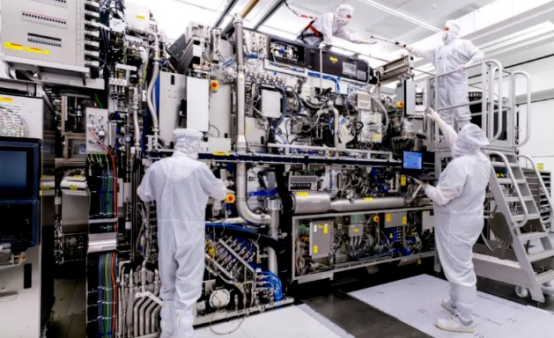
Why Precision Ceramics Matter in Semiconductor Equipment
Modern semiconductor equipment operates under extremely demanding conditions:
- High vacuum environments
- Воздействие на плазму
- Коррозионные технологические газы
- Ultra-high cleanliness requirements
- Rapid thermal cycling
- Nanometer-level precision motion
Traditional metallic materials often struggle under these conditions due to contamination risks, thermal deformation, or chemical instability.
Advanced ceramic materials provide critical advantages:
- High purity and low contamination
- Отличная износостойкость
- Выдающаяся плазмостойкость
- Низкое тепловое расширение
- High rigidity and dimensional stability
- Превосходные диэлектрические свойства
- Superior heat resistance
- Низкое образование частиц
As a result, precision ceramic components are extensively used inside semiconductor process chambers and wafer handling systems.
Precision Ceramics in Front-End Semiconductor Manufacturing Equipment
1. Lithography Systems
High-end lithography machines require ultra-precise motion systems and structurally stable materials to achieve nanometer-scale patterning accuracy.
Typical ceramic components include:
- Электростатические патроны (ESC)
- Вакуумные патроны
- Motion stages
- Направляющие
- Worktables
- Mask stages
- Cooling plates
- Structural blocks
- Mirror support structures
Electrostatic Chuck (ESC)
Electrostatic chucks are among the most critical ceramic components in semiconductor manufacturing. They are used to securely hold and transfer wafers during plasma and vacuum-based processes such as:
- Плазменное травление
- Chemical vapor deposition (CVD)
- Ионная имплантация
Common Ceramic Materials
- Глинозем (Al₂O₃)
- Нитрид кремния (Si₃N₄)
Manufacturing Challenges
- Complex internal structures
- High-purity raw material preparation
- Precision sintering control
- Ultra-flat surface machining
- Embedded electrode integration
Precision Motion Stages
Lithography stages must achieve extremely high speed and positioning accuracy while minimizing deformation during rapid acceleration.
Material Requirements
- Высокая удельная жесткость
- Низкая плотность
- Низкое тепловое расширение
- Отличная стабильность размеров
Common Ceramic Materials
- Cordierite ceramics
- Silicon carbide (SiC)
Silicon carbide is especially attractive due to its lightweight structure, high rigidity, and excellent thermal stability.
2. Etching Equipment
Etching systems transfer circuit patterns from masks onto wafers and operate under highly corrosive plasma environments.
Ceramic components commonly used include:
- Process chambers
- Viewports
- Газораспределительные пластины
- Форсунки
- Фокусировочные кольца
- Изолирующие кольца
- Chamber covers
- Электростатические патроны
Etching Chamber Components
As device geometries continue shrinking, contamination control becomes increasingly critical. Ceramic materials have gradually replaced metals in many chamber applications.
Key Material Requirements
- Сверхвысокая чистота
- Низкий уровень металлического загрязнения
- Отличная плазмостойкость
- High density and low porosity
- Fine grain structure
- Stable dielectric properties
- Хорошая обрабатываемость
Common Ceramic Materials
- Quartz (SiO₂)
- Silicon carbide (SiC)
- Нитрид алюминия (AlN)
- Глинозем (Al₂O₃)
- Нитрид кремния (Si₃N₄)
- Yttria (Y₂O₃)
Gas Distribution Plates (Shower Heads)
Gas distribution plates contain hundreds or thousands of precision micro-holes designed to evenly distribute process gases across wafer surfaces.
Uniform gas flow directly impacts:
- Film thickness uniformity
- Etching consistency
- Урожайность
- Стабильность процесса
Technical Challenges
- Micro-hole dimensional consistency
- Burr-free internal surfaces
- Ultra-clean machining
- Устойчивость к коррозии
- High flatness
Common Ceramic Materials
- CVD Silicon Carbide (CVD-SiC)
- Alumina ceramics
- Silicon nitride ceramics
Focus Rings
Focus rings help maintain uniform plasma distribution around wafers during plasma etching processes.
Traditional conductive silicon rings suffer from rapid fluorine plasma erosion, resulting in short operational lifetimes.
Silicon carbide offers:
- Similar electrical conductivity to silicon
- Превосходная плазмостойкость
- Более длительный срок службы
Common Material
- Silicon carbide (SiC)
3. Thin-Film Deposition Equipment
Both PVD and CVD systems extensively utilize precision ceramic components due to their thermal and plasma stability.
Типичные компоненты включают:
- Электростатические патроны
- Керамические нагреватели
- Газораспределительные пластины
- Вкладыши для камер
Керамические нагреватели
Ceramic heaters directly contact wafers and provide stable, uniform process temperatures during deposition.
These components are essential for:
- Temperature uniformity
- Thin-film quality
- Process repeatability
Common Ceramic Materials
- Нитрид алюминия (AlN)
- Глинозем (Al₂O₃)
Aluminum nitride is especially favored because of its high thermal conductivity and electrical insulation properties.
Precision Ceramics in Back-End Semiconductor Processes
1. CMP (Chemical Mechanical Polishing) Equipment
CMP systems use ceramic materials in:
- Полировальные пластины
- Держатели пластин
- Вакуумные патроны
- Calibration platforms
- Robotic transfer arms
Ceramic materials provide excellent dimensional stability and wear resistance during prolonged polishing operations.
2. Wafer Dicing and Packaging Equipment
Key Ceramic Components
Diamond-Ceramic Composite Dicing Blades
- High cutting speed
- Minimal wafer chipping
- Превосходная износостойкость
Ceramic Bonding Heads
- Aluminum nitride ceramics
- Высокая теплопроводность
- Precise temperature uniformity
Ceramic Packaging Substrates
- LTCC (Low Temperature Co-fired Ceramics)
- Fine wiring capability
- High-frequency signal support
Ceramic Capillary Tools
Used in wire bonding processes.
Common Materials
- Alumina ceramics
- Zirconia toughened alumina (ZTA)
3. Semiconductor Probe Stations and Test Equipment
Key Components
Ceramic Interposer Substrates
- Beryllium oxide (BeO)
- Нитрид алюминия (AlN)
High-Frequency Test Fixtures
- Aluminum nitride ceramics
These materials support high-frequency signal transmission while maintaining thermal stability.
Ceramic Components in Wafer Handling and Clean Environments
1. Wafer Transfer Robots
Semiconductor robotic systems require:
- Высокая точность
- Низкое образование частиц
- Long operational lifetime
- Совместимость с вакуумом
Key Ceramic Components
Robotic Arms
Common Materials
- Alumina ceramics
- Silicon carbide ceramics
Joint Bearings
Common Materials
- Zirconia ceramic balls
Преимущества
- Extremely low friction coefficient
- Длительный срок службы
- Отличная износостойкость
End Effectors / Wafer Fingers
Common Material
- Silicon carbide ceramics
Performance Advantages
- Устойчивость к высоким температурам
- Сверхнизкое выделение частиц
- Отличная стабильность размеров
2. Ultra-Pure Water and Gas Delivery Systems
Ceramic materials are also critical in chemical delivery systems.
Typical Components
- Valve sealing parts
- Pipe liners
- Corrosion-resistant flow components
Common Materials
- Silicon nitride ceramics
- High-density alumina ceramics
These materials offer excellent resistance to corrosive chemicals such as hydrofluoric acid.
Key Advanced Ceramic Materials Used in Semiconductor Equipment
| Керамический материал | Основные преимущества | Типовые применения |
|---|---|---|
| Глинозем (Al₂O₃) | Insulation, wear resistance | ESCs, insulators, robot arms |
| Нитрид алюминия (AlN) | Высокая теплопроводность | Ceramic heaters, substrates |
| Карбид кремния (SiC) | Plasma resistance, rigidity | Focus rings, stages, wafer fingers |
| Нитрид кремния (Si₃N₄) | Strength, thermal shock resistance | Structural parts, seals |
| Цирконий (ZrO₂) | Высокая прочность | Bearings, wear components |
| Quartz (SiO₂) | Высокая чистота | Chambers, furnace tubes |
| Yttria (Y₂O₃) | Plasma corrosion resistance | Chamber coatings |
| Нитрид бора (BN) | Thermal stability, lubrication | Insulators, thermal components |
Future Trends in Semiconductor Ceramic Components
As semiconductor manufacturing continues evolving toward:
- Передовые технологические узлы
- AI chips
- 3D packaging
- Широкополосные полупроводники
- High-power devices
precision ceramic components will require:
- Higher purity
- Better plasma resistance
- Larger dimensions
- Lower defect density
- More complex geometries
- Ultra-precision machining
- Усовершенствованная технология обработки поверхности
Advanced ceramics are rapidly becoming one of the foundational technologies supporting future semiconductor equipment innovation.
Заключение
Precision ceramic components are essential throughout semiconductor manufacturing equipment, from lithography and plasma etching systems to wafer handling robots and packaging equipment.
Their unique combination of:
- Высокая чистота
- Термическая стабильность
- Сопротивление плазмы
- Механическая прочность
- Электрическая изоляция
- Низкий уровень загрязнения
makes advanced ceramics indispensable for achieving the precision, reliability, and cleanliness required in modern semiconductor production.
As semiconductor technology advances, the importance of high-performance ceramic materials and ultra-precision ceramic manufacturing will continue to grow.

