As semiconductor technology continues to evolve toward smaller nodes, higher integration density, and more complex manufacturing processes, the demand for advanced materials inside semiconductor equipment has increased dramatically. Modern semiconductor fabrication environments require materials capable of withstanding extreme temperatures, corrosive plasma exposure, ultra-clean vacuum conditions, and high mechanical stress while maintaining dimensional stability and contamination control.
Among the many material solutions available today, advanced ceramics have become indispensable in semiconductor manufacturing equipment due to their exceptional combination of mechanical, thermal, electrical, and chemical properties.
From wafer handling systems and etching chambers to deposition equipment and thermal processing furnaces, advanced ceramic components are widely used throughout the semiconductor production chain.
Why Advanced Ceramics Are Essential in Semiconductor Equipment
Semiconductor manufacturing equipment is becoming increasingly precise and sophisticated. Conventional metallic materials often struggle under the harsh conditions found in plasma processing, high-temperature thermal cycling, and chemically aggressive environments.
Advanced ceramics provide several critical advantages:
- Extremely high hardness and wear resistance
- Excellent electrical insulation
- Outstanding thermal stability
- Low thermal expansion
- Superior corrosion resistance
- Low particle generation
- High dimensional stability in vacuum environments
- Resistance to plasma erosion
Because of these characteristics, precision ceramic components are extensively used in:
- Wafer handling systems
- Etching equipment
- Lithography systems
- Chemical vapor deposition (CVD) equipment
- Physical vapor deposition (PVD) chambers
- Ion implantation systems
- Diffusion and oxidation furnaces
- CMP (Chemical Mechanical Polishing) equipment
In many semiconductor tools, advanced ceramic components account for a significant portion of the core functional materials and directly influence process stability, yield, and equipment lifetime.
Technical Challenges of Semiconductor Ceramic Components
To meet semiconductor industry requirements, advanced ceramic materials must satisfy three major technical demands:
1. Material Performance Requirements
Ceramic materials must maintain stable performance under:
- High temperatures
- Mechanical stress
- Plasma exposure
- Acid and alkali corrosion
- High-frequency electrical environments
- Thermal shock conditions
This requires an optimized balance of mechanical, thermal, dielectric, and chemical properties.
2. Precision Machining of Hard and Brittle Materials
Advanced ceramics are notoriously difficult to machine due to their high hardness and brittleness. Semiconductor equipment requires ultra-high dimensional accuracy, tight tolerances, and complex geometries, making precision machining one of the industry’s biggest challenges.
3. Ultra-Clean Surface Treatment
Many ceramic components are located near or directly in contact with semiconductor wafers. Therefore, strict control of:
- Metal ion contamination
- Surface roughness
- Particle generation
- Surface defects
is essential after machining and polishing processes.
Major Advanced Ceramic Materials Used in Semiconductors
1. Alumina (Al₂O₃)
Key Properties
- High hardness
- Excellent wear resistance
- Strong electrical insulation
- High-temperature resistance
- Excellent chemical stability
Typical Applications
- Wafer boats
- Electrical insulators
- CMP components
- Semiconductor packaging substrates
Alumina remains one of the most widely used engineering ceramics because of its balanced performance and cost-effectiveness.
2. Aluminum Nitride (AlN)
Key Properties
- Extremely high thermal conductivity
- Low thermal expansion coefficient
- Excellent electrical insulation
- Good thermal shock resistance
Typical Applications
- Semiconductor packaging substrates
- Heat sinks
- High-power electronic devices
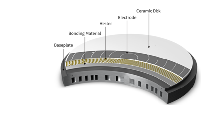
- Thin-film deposition heaters
Aluminum nitride is especially valuable in thermal management applications where rapid heat dissipation is critical.
3. Silicon Carbide (SiC)
Key Properties
- Ultra-high hardness
- Excellent high-temperature stability
- High thermal conductivity
- Outstanding corrosion resistance
- Superior plasma resistance
Typical Applications
- Etching chamber components
- Wafer susceptors
- High-temperature heaters
- Wafer handling components
- Power semiconductor substrates
Silicon carbide has become one of the most important materials in advanced semiconductor processing, especially in plasma-intensive environments.
4. Silicon Nitride (Si₃N₄)
Key Properties
- High mechanical strength
- Excellent fracture toughness
- Superior thermal shock resistance
- Outstanding wear resistance
Typical Applications
- Structural components
- Semiconductor carrier systems
- High-reliability packaging materials
- Thermal management components
Silicon nitride is widely used where both strength and reliability are required under severe operating conditions.
5. Zirconia (ZrO₂)
Key Properties
- High fracture toughness
- Excellent wear resistance
- Strong chemical stability
- Good high-temperature performance
Typical Applications
- CMP components
- Wear-resistant semiconductor parts
- High-temperature sensors
Thanks to its transformation toughening mechanism, zirconia offers superior resistance to crack propagation compared with many other ceramics.
6. Beryllium Oxide (BeO)
Key Properties
- Extremely high thermal conductivity
- Excellent electrical insulation
- Low dielectric constant
- High-temperature stability
Typical Applications
- High-power semiconductor packaging
- RF and microwave substrates
- Thermal management systems
Beryllium oxide combines metal-like thermal conductivity with ceramic insulation properties, making it highly effective in specialized electronic applications.
7. Piezoelectric Ceramics (PZT)
Key Properties
- Excellent piezoelectric response
- High sensitivity
- Fast actuation capability
- Good temperature stability
Typical Applications
- Precision positioning systems
- Semiconductor sensors
- Acoustic wave devices
- Precision actuators
Piezoelectric ceramics play an important role in ultra-precision motion control systems used in semiconductor manufacturing.
8. Quartz Ceramic (SiO₂)
Key Properties
- Ultra-high purity
- Very low thermal expansion
- Excellent thermal resistance
- Outstanding chemical stability
Typical Applications
- Diffusion furnace tubes
- Lithography system components
- Wafer carriers
Quartz materials are especially important in ultra-clean and high-temperature semiconductor environments.
9. Boron Nitride (BN)
Key Properties
- High thermal conductivity
- Low dielectric constant
- Excellent lubricating properties
- Outstanding thermal shock resistance
Typical Applications
- High-temperature insulation
- Thermal management components
- Lubricating parts in semiconductor equipment
Boron nitride is particularly useful in applications requiring both thermal stability and non-reactive behavior.
The Future of Advanced Ceramics in Semiconductor Manufacturing
As semiconductor manufacturing advances toward:
- Smaller process nodes
- Higher wafer throughput
- More aggressive plasma processing
- Advanced packaging technologies
- Wide-bandgap semiconductors
the performance requirements for ceramic materials will continue to increase.
Future trends include:
- Higher purity ceramic materials
- Improved plasma-resistant coatings
- Ultra-low particle generation surfaces
- Larger and more complex ceramic structures
- Advanced composite ceramic systems
- Greater integration with AI-driven manufacturing equipment
Advanced ceramics are no longer merely supporting materials — they have become critical enabling technologies for next-generation semiconductor manufacturing.
Conclusion
Advanced ceramic materials have become fundamental to modern semiconductor equipment due to their unmatched combination of thermal stability, electrical insulation, mechanical strength, and chemical resistance.
Materials such as alumina, aluminum nitride, silicon carbide, silicon nitride, zirconia, quartz, and boron nitride each provide unique advantages for specific semiconductor manufacturing processes.
As the semiconductor industry continues to pursue higher precision, higher efficiency, and greater reliability, advanced ceramics will remain at the center of technological innovation and equipment development.