
A ceramic wafer end effector—also called a wafer handling blade, robot blade or wafer transfer arm—is the part of a semiconductor robot that directly supports and transfers wafers between process chambers, load ports, aligners, inspection stations and wafer carriers.
Although its geometry may appear simple, the end effector directly affects wafer positioning accuracy, transfer speed, particle generation, electrostatic discharge risk and equipment uptime.
A successful ceramic wafer end effector must combine several requirements:
- Low moving mass
- Высокая жесткость
- Precise dimensions
- Controlled flatness
- Stable wafer support
- Низкое образование частиц
- Smooth, wear-resistant surfaces
- Reliable vacuum performance
- Thermal and chemical compatibility
- Suitable electrical resistivity
Ceramic end effectors are used because advanced ceramics can provide dimensional precision, thermal stability, abrasion resistance and low-contamination wafer contact. Some wafer-handling systems also use ESD-safe ceramic materials to dissipate accumulated static charge.
This guide explains how material, weight, stiffness, flatness, surface condition and vacuum design should be considered when developing a custom ceramic wafer end effector.
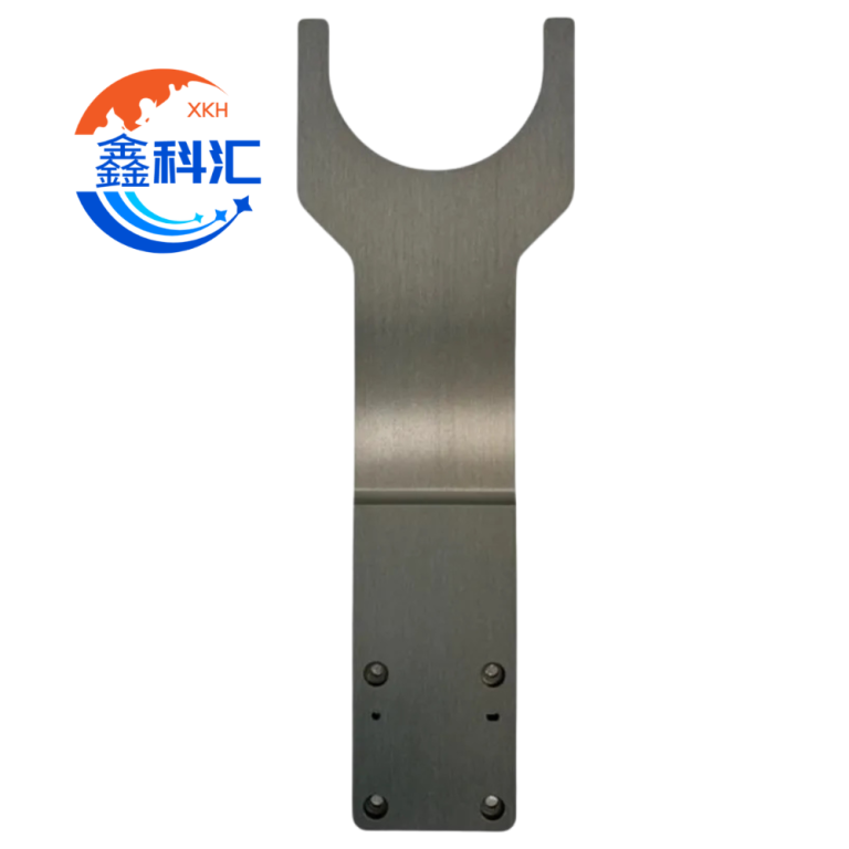
What Does a Wafer End Effector Do?
The end effector acts as the “hand” of a wafer transfer robot.
Its typical functions include:
- Entering a wafer cassette or process chamber
- Moving beneath a wafer without contact with adjacent wafers
- Lifting the wafer from pins or a support ring
- Holding the wafer during robot acceleration
- Maintaining wafer orientation during transfer
- Placing the wafer accurately on a chuck or process stage
- Releasing the wafer without sliding or sticking
The end effector may support the wafer using:
- Backside vacuum
- Passive gravity support
- Edge gripping
- Bernoulli lift
- Mechanical clamps
- A combination of vacuum and mechanical positioning features
Vacuum ceramic end effectors are common where stable backside support and controlled robot motion are required.
The Four Main Design Priorities
The performance of a ceramic wafer handling blade can be evaluated through four closely related design priorities.
Материал
The material determines stiffness, density, thermal expansion, electrical behavior, wear resistance and compatibility with the process environment.
Вес
End-effector mass affects robot acceleration, settling time, vibration, motor load and achievable throughput.
Flatness
Flatness influences the distribution of wafer support, vacuum sealing, wafer tilt and handoff accuracy.
Particle control
Particle performance depends on material purity, surface finish, wear, contact geometry, cleaning and the way the wafer slides onto or off the blade.
Optimizing only one parameter can create problems elsewhere. For example, reducing thickness lowers weight but can also increase deflection. Increasing the contact area may improve support but can trap more particles beneath the wafer.
Ceramic Material Selection
There is no single ceramic material that is best for every wafer end effector.
The correct selection depends on:
- Wafer diameter
- Robot speed and acceleration
- End-effector length
- Рабочая температура
- Chemical environment
- Required electrical resistivity
- Allowed particle level
- Maximum allowable weight
- Impact and handling risk
- Cleaning process
- Cost and production quantity
Common candidate materials include alumina, silicon carbide, silicon nitride, aluminum nitride, zirconia and ESD-safe ceramic compositions.
Alumina Ceramic End Effectors
High-purity alumina is one of the most established materials for semiconductor ceramic components and wafer transfer parts.
К числу типичных преимуществ относятся:
- Высокая твердость
- Хорошая стабильность размеров
- Сильная электрическая изоляция
- Хорошая износостойкость
- Availability in multiple purity grades
- Mature precision-machining processes
- Good resistance to many process chemicals
Ferrotec lists high-purity alumina grades with density around 3.93–3.95 g/cm³ and Young’s modulus around 375–380 GPa. Its alumina products are used for semiconductor equipment and wafer transfer components. Exact properties depend on purity, additives and manufacturing method.
Alumina is often suitable for:
- Standard atmospheric wafer-transfer robots
- Electrically insulating blades
- Общая обработка пластин
- Cost-sensitive production equipment
- Moderate-temperature processes
Potential limitations include:
- Greater density than some SiC-based options
- Higher thermal expansion than SiC
- Brittle behavior around sharp corners or thin sections
- Limited static dissipation unless a conductive or ESD-safe grade is selected
Silicon Carbide End Effectors
Silicon carbide is attractive when high stiffness, low weight, thermal stability and wear resistance are important.
A representative dense SiC grade listed by Ferrotec has:
- Density around 3.1 g/cm³
- Young’s modulus around 400 GPa
- Thermal conductivity around 130 W/m·K
- Thermal expansion around 3.9 × 10⁻⁶/°C from room temperature to 500°C
These values give SiC a high stiffness-to-weight ratio and relatively low thermal expansion.
Potential advantages include:
- High specific stiffness
- Low bending under robot acceleration
- Хорошая стабильность размеров
- Высокая твердость и износостойкость
- Good thermal conductivity
- Lower thermal expansion than alumina
- Suitability for long or thin blade geometries
SiC may be preferred for:
- High-speed wafer-transfer robots
- Long-reach end effectors
- Large wafers
- High-precision inspection equipment
- Temperature-variable environments
- Applications requiring rapid robot settling
Not all SiC grades have the same electrical, purity or surface characteristics. Sintered SiC, reaction-bonded SiC, Si-SiC and CVD SiC should not be treated as interchangeable materials.
Silicon–Silicon Carbide Composite Materials
Si-SiC composites can provide a useful combination of low density, stiffness, low thermal expansion and thermal conductivity.
Representative Si-SiC materials listed by Ferrotec have densities of approximately 2.8–3.0 g/cm³ and Young’s modulus values of approximately 280–330 GPa. The manufacturer identifies lightweight construction, stiffness and low thermal expansion as benefits for semiconductor and precision equipment components.
These materials may be considered for:
- Lightweight robot structures
- Large end effectors
- Высокоскоростное прецизионное перемещение
- Applications where mechanical damping is valuable
However, exposed free silicon, material purity and surface finishing must be reviewed for the intended process environment.
Aluminum Nitride End Effectors
Aluminum nitride combines electrical insulation with relatively high thermal conductivity.
Representative AlN grades have density around 3.24–3.31 g/cm³, Young’s modulus around 320 GPa and thermal conductivity ranging from approximately 80 to 150 W/m·K, depending on the grade.
AlN may be considered when the end effector requires:
- Электрическая изоляция
- Heat spreading
- Lower thermal expansion than alumina
- Compatibility with elevated-temperature wafers
- Controlled temperature distribution
AlN is generally more specialized and can be more sensitive to manufacturing, moisture exposure and cleaning chemistry than alumina. Its use should therefore be based on a clearly defined thermal requirement rather than material reputation alone.
Silicon Nitride End Effectors
Silicon nitride offers high strength, impact resistance and thermal-shock performance.
A representative grade listed by Ferrotec has density around 3.25 g/cm³, Young’s modulus around 285 GPa and high bending strength compared with many common structural ceramics.
It may be useful where the end effector is exposed to:
- Higher mechanical shock
- Accidental contact
- Rapid temperature changes
- Thin features with elevated fracture risk
- Repeated loading and unloading
Its lower elastic modulus than some SiC and alumina grades means that geometry still needs to be optimized for stiffness.
Zirconia End Effectors
Zirconia is known for high fracture toughness, wear resistance and mechanical strength.
However, it is considerably denser than alumina or SiC. A representative zirconia grade has density around 5.98 g/cm³ and Young’s modulus around 245 GPa.
This combination generally makes zirconia less attractive for a complete high-speed robot blade because it adds moving mass without providing the highest stiffness.
Zirconia can still be valuable for:
- Local wear inserts
- Contact pads
- Edge-gripping components
- Small mechanical features
- Parts requiring elevated fracture toughness
Using zirconia only at high-wear contact points may be more efficient than manufacturing the entire end effector from zirconia.
ESD-Safe Ceramic Materials
A highly insulating ceramic can allow electrostatic charge to remain on the end effector or wafer.
Depending on the equipment and wafer state, uncontrolled charge can contribute to:
- Электростатическое притяжение
- Particle attraction
- Unstable wafer release
- Damage to sensitive devices
- Electrostatic discharge events
ESD-safe ceramics are engineered with controlled resistivity so accumulated charge can dissipate rather than remaining isolated. CoorsTek specifically identifies ESD-safe ceramic compositions for wafer-processing equipment and end-effector construction.
The RFQ should specify whether the end effector must be:
- Electrically insulating
- Static dissipative
- Conductive
- Grounded through the robot
- Tested at a particular temperature and humidity
“ESD safe” should not be used as a general description without a target resistance or resistivity range.
Comparing Common End-Effector Materials
Typical published values illustrate why density alone is not sufficient for material selection.
| Материал | Typical Density | Typical Young’s Modulus | General Design Characteristic |
|---|---|---|---|
| Глинозем | 3.93–3.95 g/cm³ | 375–380 GPa | Mature, hard and electrically insulating |
| Dense SiC | About 3.1 g/cm³ | About 400 GPa | High specific stiffness and low thermal expansion |
| AlN | 3.24–3.31 g/cm³ | About 320 GPa | Electrically insulating with high thermal conductivity |
| Silicon nitride | About 3.25 g/cm³ | About 285 GPa | High strength and thermal-shock resistance |
| Цирконий | About 5.98 g/cm³ | About 245 GPa | Tough and wear-resistant, but relatively heavy |
| Si-SiC composite | 2.8–3.0 g/cm³ | 280–330 GPa | Lightweight with good thermal stability |
These are representative supplier values rather than universal specifications. Ceramic properties vary with grade, purity, porosity, grain structure, forming process and part geometry.
Why End-Effector Weight Matters
A wafer robot must accelerate, decelerate and precisely position the combined mass of:
- Robot arm
- End effector
- Mounting hardware
- Vacuum tubing or internal channels
- Wafer
The inertial force increases with mass and acceleration:
F = m × a
Reducing end-effector mass can therefore reduce:
- Motor torque demand
- Robot vibration
- Structural loading
- Settling time
- Bearing and drive wear
- Energy consumption
It may also allow:
- Faster transfer cycles
- Higher acceleration
- Improved positioning repeatability
- Greater payload margin
However, simply making the blade thinner is not always a safe solution.
Weight Reduction vs Stiffness
A long end effector behaves approximately like a cantilever beam. Its vertical deflection is strongly influenced by:
- Unsupported length
- Material elastic modulus
- Cross-sectional geometry
- Wafer load
- Robot acceleration
- Location of the wafer center of gravity
For a simplified cantilever model, tip deflection increases approximately with the cube of length:
δ ∝ FL³/EI
Где:
- δ is deflection
- F is applied load
- L is unsupported length
- E is Young’s modulus
- I is the cross-sectional moment of inertia
This relationship explains why a small increase in reach can produce a large increase in deflection.
Weight reduction should therefore focus on efficient geometry rather than uniform thickness reduction.
Useful strategies include:
- Removing material close to the neutral axis
- Adding shallow reinforcing ribs
- Increasing section depth in non-contact regions
- Tapering the blade toward the wafer end
- Reducing unnecessary mounting mass
- Using lightweight high-stiffness materials
- Shortening unsupported length where possible
- Integrating vacuum channels without weakening critical sections
Open pockets and ribs must be designed with generous ceramic radii to avoid creating stress concentrations.
Specific Stiffness
Specific stiffness is the ratio of elastic modulus to density:
Specific stiffness = E/ρ
A material with high specific stiffness can provide greater resistance to deflection for a given mass.
Based on representative supplier values, dense SiC generally offers a higher modulus-to-density ratio than alumina or zirconia. This is one reason SiC is attractive for long, lightweight, high-speed wafer-handling structures.
Material selection should still consider machining, purity, electrical behavior, thermal requirements and impact risk.
End-Effector Flatness
Flatness is a critical specification, but the drawing must clearly define which surface and area are being controlled.
Possible flatness requirements include:
- Overall blade flatness
- Wafer-support land flatness
- Vacuum-pad flatness
- Flatness of multiple support pads as a common plane
- Flatness relative to the mounting interface
- Loaded flatness under wafer weight
- Dynamic flatness during acceleration
A generic note such as “flatness: 0.02 mm” may be insufficient unless the datum structure and measurement area are identified.
Flatness vs Parallelism
Flatness controls the shape of one surface.
Parallelism controls the orientation of one surface relative to another datum.
For a robot blade, both may be important:
- The wafer-support surface must be flat.
- The support surface may also need to be parallel to the robot mounting plane.
- Vacuum pads may need to lie in the same plane.
- The mounting holes must position the blade without introducing twist.
A blade can have a flat support surface but still hold the wafer at an angle if the support plane is not parallel to the mounting datum.
Static Flatness vs Installed Flatness
A ceramic end effector can meet its free-state flatness specification and still distort after installation.
Potential causes include:
- Uneven bolt torque
- An inaccurate metal adapter
- Burrs beneath the mounting surface
- Over-constrained locating pins
- Thermal-expansion mismatch
- Incorrect gasket thickness
- Vacuum fittings applying mechanical stress
- Robot-arm mounting error
The qualification plan should distinguish between:
- Unmounted ceramic-part inspection
- Installed end-effector inspection
- Loaded wafer position
- Dynamic robot performance
Wafer Support Geometry
The wafer should be supported without creating excessive local stress or unstable contact.
Common support designs include:
- Three-point pads
- Multiple raised lands
- Continuous support rails
- Annular support regions
- Small ceramic bumps
- Replaceable contact inserts
- Vacuum pads with sealing lands
Three-point support
Three points define a plane and reduce the risk of rocking caused by support-height variation.
However, small pads can create higher local contact stress and may provide limited friction.
Multiple support pads
Multiple pads distribute wafer weight and vacuum force over a larger area.
Their heights must be tightly controlled. One high pad can dominate the contact and tilt the wafer.
Continuous support
Continuous lands provide a large contact area and may improve vacuum sealing.
They can also increase:
- Particle trapping
- Backside contact
- Sliding friction
- Sensitivity to surface contamination
The preferred structure depends on wafer thickness, backside condition, robot motion and contamination limits.
Vacuum End-Effector Design
A vacuum end effector must generate enough holding force to prevent wafer slip during the most demanding robot motion.
The theoretical vacuum force can be estimated as:
F = ΔP × A
Где:
- F is vacuum holding force
- ΔP is the pressure differential
- A is the effective sealed vacuum area
The practical holding force is lower because of:
- Leakage
- Incomplete sealing
- Wafer bow
- Surface particles
- Pressure loss in internal channels
- Vacuum-line restrictions
- Local pad deformation
The design should also verify lateral slip resistance, which depends on the normal force and the friction condition between the wafer and support surface.
Vacuum Port and Channel Design
Vacuum channels must provide fast, stable evacuation without weakening the ceramic blade.
Important parameters include:
- Port location
- Port diameter
- Internal channel diameter
- Channel length
- Groove width and depth
- Number of vacuum zones
- Sealing-land width
- Vacuum-pad area
- Allowable leakage rate
- Required gripping time
- Required release time
Sharp internal corners should be avoided because ceramics are sensitive to tensile stress concentration.
Blind passages must also be designed so that they can be cleaned and inspected.
Vacuum Pad Location
Vacuum pads should normally be positioned to:
- Hold the wafer near stable support regions
- Avoid excessive wafer bending
- Prevent rotation
- Maintain clearance from wafer edges
- Minimize the effect of wafer bow
- Support repeatable loading
A single central vacuum pad can allow wafer rotation if lateral friction is insufficient.
Widely separated pads may improve rotational stability but can be more sensitive to wafer bow and pad-height variation.
The final layout should be validated using the actual wafer thickness, bow, backside film and robot acceleration.
Контроль частиц
Particle control is not determined only by ceramic purity.
Particles can be generated by:
- Surface wear
- Edge chipping
- Wafer sliding
- Abrasion at mounting interfaces
- Contaminated vacuum channels
- Loose inserts
- Poor cleaning
- Incompatible coatings
- Repeated impact with cassette components
- Residue left after machining or lapping
CoorsTek describes wafer-handling end effectors as requiring smooth, abrasion-resistant surfaces to transfer wafers without producing particulate contamination.
Шероховатость поверхности
The lowest possible roughness is not always the correct requirement.
An extremely smooth ceramic surface may:
- Increase the real contact area
- Increase adhesion
- Make wafer release less predictable
- Increase sensitivity to moisture films
- Increase the effect of electrostatic attraction
A rougher surface may:
- Reduce real contact area
- Improve release
- Increase localized stress
- Scratch the wafer backside
- Generate particles through asperity wear
The target roughness must be matched to the wafer backside, contact-pad design and release method.
The drawing should identify whether the surface requirement applies to:
- All ceramic surfaces
- Wafer-contact pads only
- Vacuum sealing lands
- Mounting surfaces
- Non-contact exterior surfaces
Edge and Corner Design
Ceramic edge quality has a direct influence on handling durability and particle generation.
Sharp ceramic edges are vulnerable to:
- Chipping during cleaning
- Impact damage during installation
- Particle shedding
- Stress concentration
- Damage to nearby equipment
Recommended drawing practices include:
- Defining edge breaks
- Adding radii at internal corners
- Avoiding abrupt thickness changes
- Removing knife-edge features
- Protecting exposed tips
- Separating wafer-contact edges from fragile external edges
“Deburr all edges” is not precise enough for a ceramic component. Edge radius, chamfer size or maximum edge-chip allowance should be specified where critical.
Wafer Sliding and Contact Motion
Some end effectors move directly beneath a wafer before lifting it. Any height mismatch can cause the blade to slide against the wafer backside.
Sliding can produce:
- Backside scratches
- Ceramic wear
- Particle transfer
- Wafer displacement
- Edge damage
The equipment design should minimize sliding by coordinating:
- Blade height
- Lift-pin height
- Robot Z-position
- Wafer bow
- Cassette-slot geometry
- Approach speed
When sliding cannot be avoided, contact-pad material and surface finish become especially important.
Cleaning and Cleanliness
A custom end effector should be designed around the intended cleaning process.
Possible cleaning methods include:
- Ultrasonic cleaning
- Megasonic cleaning
- High-purity water rinsing
- Solvent cleaning
- Acid or alkaline cleaning
- Plasma cleaning
- Clean dry-air or nitrogen blow-off
- Cleanroom baking
The supplier should confirm that the ceramic grade, bonding materials, inserts and markings are compatible with the specified cleaning chemistry and temperature.
Particle-control requirements may include:
- Cleaning procedure
- Final rinse-water quality
- Drying method
- Packaging environment
- Double cleanroom bagging
- Particle inspection
- Ionic contamination testing
- Nonvolatile residue requirements
Термическая стабильность
The end effector may transfer wafers that are hotter or colder than the surrounding robot.
Temperature changes can cause:
- Blade expansion
- Wafer-position shift
- Vacuum-pad misalignment
- Temporary bending
- Stress at metal-to-ceramic joints
- Changes in electrical resistivity
- Changes in vacuum sealing
Materials with low thermal expansion and high thermal conductivity may reduce thermal gradients and positioning drift.
SiC and Si-SiC materials typically have lower thermal expansion than alumina, while AlN and SiC provide higher thermal conductivity than standard alumina grades.
The designer should define:
- Wafer pickup temperature
- Maximum blade temperature
- Heating and cooling rate
- Robot mounting temperature
- Acceptable positioning drift
- Thermal-cycle quantity
Metal-to-Ceramic Mounting
Ceramic end effectors are usually attached to a metal robot arm or adapter.
The joint must accommodate differences in:
- Тепловое расширение
- Surface flatness
- Stiffness
- Manufacturing tolerance
- Bolt preload
Common mounting approaches include:
- Through bolts
- Clamping plates
- Bonded inserts
- Threaded metal inserts
- Kinematic locating features
- Precision dowel pins
Directly tightening a bolt against an unsupported ceramic section can create high local stress.
Mounting features should distribute load and avoid over-constraining the ceramic.
Common Failure Modes
The wafer slips during acceleration
Possible causes include:
- Insufficient vacuum force
- Vacuum leakage
- Poor pad location
- Low friction
- Excessive robot acceleration
- Contaminated support pads
- Warped wafer
The blade vibrates after motion
Possible causes include:
- Excessive blade length
- Insufficient section stiffness
- High moving mass
- Low-stiffness mounting
- Poor robot-control tuning
- An unsuitable material-to-geometry combination
The wafer is tilted
Possible causes include:
- Support-pad height variation
- Poor mounting parallelism
- Blade warpage
- Particles on a support pad
- Incorrect robot calibration
- Uneven vacuum sealing
Particle counts increase over time
Possible causes include:
- Contact-pad wear
- Edge chipping
- Wafer sliding
- Contaminated vacuum passages
- Loose inserts
- Cleaning damage
- Abrasion against cassette slots
The ceramic blade cracks near the mounting holes
Possible causes include:
- Excessive bolt torque
- Sharp internal corners
- Hole-position error
- Metal-adapter distortion
- Thermal-expansion mismatch
- Insufficient material around the hole
- Impact during installation
The wafer does not release consistently
Possible causes include:
- Residual vacuum
- Slow venting
- Excessively smooth contact surfaces
- Moisture adhesion
- Static charge
- Blocked release channels
- Wafer bow
Design and Validation Process
Step 1: Define the wafer
Provide:
- Wafer material
- Diameter
- Thickness
- Вес
- Bow and warp
- Edge profile
- Backside coating
- Allowed contact regions
- Maximum backside scratch or particle limit
Step 2: Define robot motion
Provide:
- Maximum linear acceleration
- Maximum rotational acceleration
- Transfer speed
- End-effector reach
- Cycle time
- Required settling time
- Wafer orientation
- Emergency-stop load case
Step 3: Select the holding method
Compare:
- Vacuum holding
- Passive support
- Edge grip
- Mechanical clamp
- Bernoulli handling
Step 4: Select the ceramic
Evaluate:
- Плотность
- Elastic modulus
- Strength
- Вязкость разрушения
- Тепловое расширение
- Теплопроводность
- Electrical resistivity
- Чистота
- Wear behavior
- Machinability
- Стоимость
Step 5: Analyze deformation and stress
Finite-element analysis should consider:
- Gravity sag
- Wafer weight
- Robot acceleration
- Vacuum force
- Mounting preload
- Emergency stop
- Thermal gradients
- Local stress around holes and channels
Step 6: Manufacture and inspect prototypes
Inspection may include:
- Dimensional report
- Support-surface flatness
- Mounting-plane parallelism
- Шероховатость поверхности
- Edge quality
- Vacuum leakage
- Airflow
- Electrical resistivity
- Material certification
Precision ceramic suppliers commonly manufacture custom components from customer drawings for semiconductor, inspection and vacuum equipment.
Step 7: Test in the equipment
Validate:
- Wafer pickup
- Wafer release
- Maximum acceleration
- Position repeatability
- Wafer tilt
- Vacuum response time
- Dynamic vibration
- Генерация частиц
- Static behavior
- Термоциклирование
- Cleaning durability
RFQ Checklist for a Custom Ceramic Wafer End Effector
An accurate quotation requires more than a simple 2D outline.
Wafer information
- Wafer diameter
- Wafer material
- Wafer thickness
- Wafer weight
- Bow and warp
- Backside film or coating
- Allowed contact area
End-effector dimensions
- Overall length
- Maximum width
- Thickness
- Wafer-center position
- Mounting-hole pattern
- Datum structure
- Clearance envelope
- Maximum allowable weight
Требования к материалам
- Глинозем
- Silicon carbide
- Silicon nitride
- Aluminum nitride
- Цирконий
- Si-SiC
- ESD-safe ceramic
- Alternative material proposals allowed or not allowed
Требования к точности
- Dimensional tolerances
- Support-pad flatness
- Mounting parallelism
- Support-pad coplanarity
- Position tolerance
- Шероховатость поверхности
- Edge radius or chamfer
Vacuum requirements
- Operating vacuum pressure
- Vacuum port type
- Port location
- Required gripping time
- Required release time
- Maximum allowable leakage
- Blow-off or venting requirement
- Number of vacuum zones
Требования к электрооборудованию
- Insulating, dissipative or conductive
- Surface resistance
- Volume resistivity
- Grounding method
- Test voltage
- Test temperature and humidity
Operating environment
- Atmospheric or vacuum operation
- Maximum temperature
- Химическое воздействие
- Воздействие на плазму
- Cleanroom class
- Cleaning method
- Maximum robot acceleration
- Expected cycle quantity
Quality documentation
- Material certificate
- Dimensional inspection report
- Flatness report
- Roughness report
- Vacuum test report
- Resistivity report
- Cleaning record
- Packaging requirement
- First article inspection
Часто задаваемые вопросы
Why are ceramics used for wafer robot blades?
Ceramics can provide high stiffness, dimensional stability, wear resistance, electrical insulation and clean wafer-contact surfaces. Appropriate ceramic selection can also reduce thermal drift and particle generation.
Is SiC always better than alumina?
No. SiC generally offers high specific stiffness, low thermal expansion and good thermal conductivity. Alumina offers mature manufacturing, electrical insulation and broad availability. The correct choice depends on motion, environment, electrical and cost requirements.
How light should an end effector be?
There is no universal target. The maximum allowable mass should be based on robot payload, acceleration, vibration, settling time and stiffness requirements.
Does a thinner blade always improve robot speed?
A thinner blade may reduce mass, but it also lowers bending stiffness and can increase vibration. Cross-sectional geometry and material stiffness must be considered together.
How should end-effector flatness be specified?
The drawing should identify the controlled surface, datum system, measurement area, edge exclusion and whether the requirement applies before or after installation.
What causes particles on ceramic end effectors?
Common causes include wafer sliding, surface wear, ceramic edge chipping, contaminated vacuum passages, loose inserts and improper cleaning.
When is ESD-safe ceramic required?
It should be considered when static buildup may attract particles, interfere with wafer release or damage sensitive devices. The required resistance or resistivity range should be specified.
Can a ceramic end effector be manufactured from an existing sample?
Reverse engineering may be possible, but a sample alone may not communicate material grade, internal channels, critical datums or electrical requirements. A drawing and operating specifications are preferred.
Заключение
Ceramic wafer end-effector design is a balance between mass, stiffness, precision and cleanliness.
The most important design principles are:
- Select material according to the complete operating environment.
- Reduce mass without sacrificing bending stiffness.
- Specify flatness together with datums and parallelism.
- Match vacuum-pad geometry to wafer bow and robot acceleration.
- Control surfaces, edges and contact motion to reduce particles.
- Define electrical behavior rather than simply requesting “ESD safe.”
- Evaluate installed and dynamic performance, not only free-state dimensions.
- Validate the final design with actual wafers and production robot motion.
A properly designed ceramic end effector can improve wafer-transfer accuracy, shorten settling time, reduce contamination and support stable operation over a large number of handling cycles.
SEO Information
SEO Title:
Ceramic Wafer End Effector Design: Material, Weight, Flatness and Particle Control
Meta Description:
Learn how to design a ceramic wafer end effector by comparing SiC, alumina and other materials for weight, stiffness, flatness, vacuum holding and particle control.
Suggested URL:/ceramic-wafer-end-effector-design-material-weight-flatness/
Primary Keyword:
ceramic wafer end effector
Secondary Keywords:
wafer handling end effector, ceramic robot blade, wafer transfer blade, SiC end effector, alumina wafer blade, vacuum end effector, semiconductor wafer handling, ESD safe ceramic, wafer robot arm
TAGS:
ceramic wafer end effector,wafer handling end effector,ceramic robot blade,wafer transfer blade,SiC end effector,alumina wafer blade,vacuum end effector,semiconductor wafer handling,ESD safe ceramic,particle control