
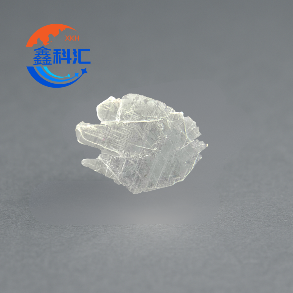

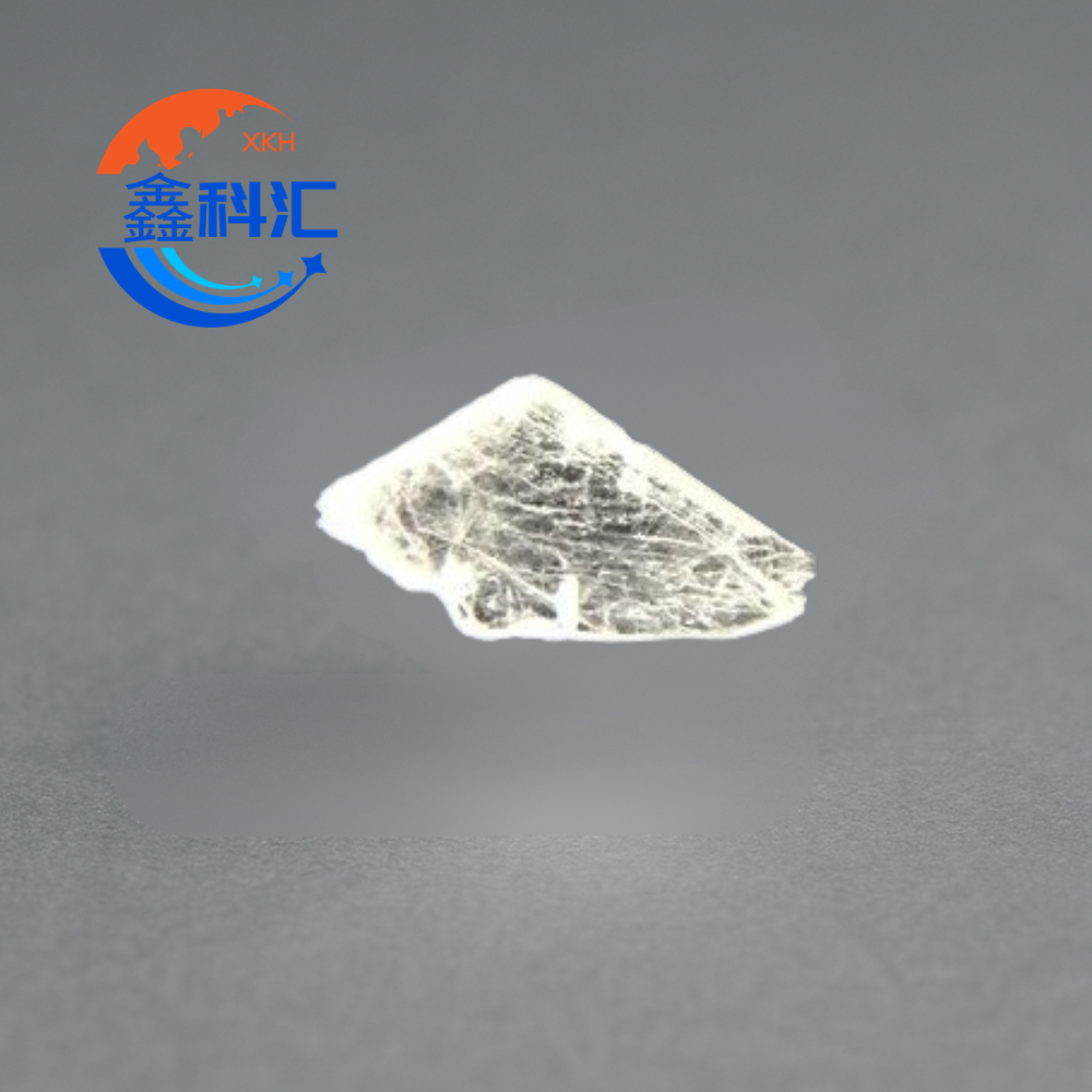

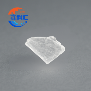
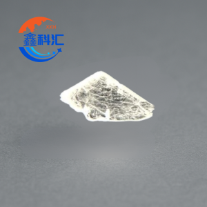
Device-Grade Hexagonal Boron Nitride (hBN) Single Crystal is an ultra-high-quality layered crystal material engineered for next-generation electronic, photonic, and quantum technologies. Produced through a proprietary atmospheric-pressure crystal growth process, these millimeter-scale single crystals exhibit exceptional structural integrity, low defect density, and outstanding dielectric and optical properties.
As one of the most important van der Waals materials, hBN serves as an ideal substrate and encapsulation layer for graphene and other two-dimensional materials. Its atomically flat surface, chemical inertness, and wide bandgap make it indispensable in the fabrication of high-performance electronic devices and advanced research platforms.
Independent studies have demonstrated that graphene devices fabricated on these crystals achieve carrier mobilities comparable to or exceeding those obtained using internationally recognized benchmark hBN materials.
제품 특징
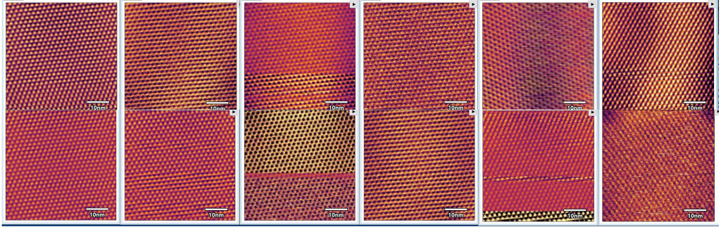
Ultra-High Crystal Quality
The material exhibits narrow Raman linewidths and large single-domain regions, indicating excellent crystal perfection and minimal structural defects.
Ideal Substrate for 2D Materials
hBN provides an atomically smooth and contamination-free interface, reducing charge scattering and improving electronic transport in graphene and other layered materials.
뛰어난 전기 절연성
With a dielectric breakdown field approaching 1.64 V/nm, hBN is widely used as a high-performance insulating layer in nanoelectronic devices.
Deep Ultraviolet Optical Properties
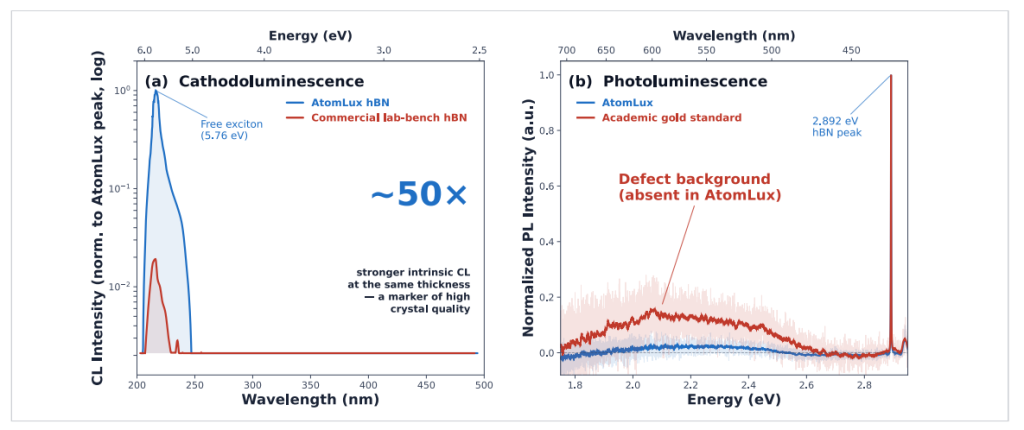
The crystal exhibits intrinsic band-edge emission near 215 nm, making it attractive for deep-UV photonics and optoelectronic research.
Large-Area Single Crystal Domains
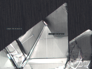
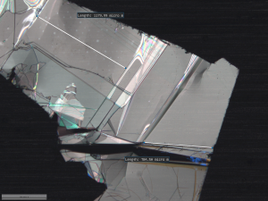
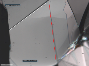
Typical crystals feature lateral dimensions exceeding 1 mm and maintain large usable regions suitable for exfoliation and device fabrication.
기술 사양
| 항목 | 사양 |
|---|---|
| 재료 | Hexagonal Boron Nitride (hBN) |
| 결정 구조 | Single Crystal |
| Grade | Device Grade |
| Growth Method | Proprietary Atmospheric-Pressure Growth |
| Crystal Form | Bulk Crystal |
| Typical Lateral Size | ≥ 1 mm |
| Surface Condition | Natural Growth Facets |
| 포장 | Chip Carrier |
| Quantity | 5–10 Crystals per Package |
전기적 특성
| 매개변수 | 일반 값 |
| Dielectric Breakdown Strength | 1.64 ± 0.06 V/nm |
Optical Properties
| 매개변수 | 일반 값 |
| UV Band-Edge Emission | ~215 nm |
| Luminescence Performance | State-of-the-Art |
| 광학 투명도 | 높음 |
Raman Characteristics
| 매개변수 | 일반 값 |
| E₂g Raman FWHM | 7.88 cm⁻¹ |
Reference Device Performance
| 매개변수 | 일반 값 |
| Graphene Mobility (300 K) | ~80,000 cm²/V·s |
| Carrier Density | 1 × 10¹² cm⁻² |
애플리케이션
Graphene Device Fabrication
hBN is the preferred substrate and encapsulation material for high-mobility graphene transistors, Hall devices, sensors, and quantum transport structures.
Van der Waals Heterostructures
The crystal is widely used in the assembly of layered heterostructures involving graphene, MoS₂, WS₂, WSe₂, and other two-dimensional materials.
Quantum Electronics
Researchers utilize device-grade hBN in studies of correlated electron systems, superconductivity, moiré materials, and quantum information technologies.
Nanophotonics
Its ability to support phonon-polaritons makes hBN an attractive material for nanoscale optical confinement and photonic device development.
Deep-UV Optoelectronics
The intrinsic ultraviolet emission characteristics of hBN enable applications in UV light sources, detectors, and advanced optical systems.
Advantages Over Conventional hBN Materials
Compared with polycrystalline boron nitride and lower-grade crystals, device-grade hBN offers:
- Larger single-crystal domains
- Lower impurity concentration
- Reduced defect density
- Higher dielectric strength
- Improved graphene carrier mobility
- Superior optical performance
- Better reproducibility for research applications
These advantages make device-grade hBN a critical material for cutting-edge semiconductor and quantum technology research.
Available Customization
Custom solutions are available based on customer requirements, including:
- Crystal size selection
- Research-grade crystal screening
- Large-domain crystal supply
- Specialized packaging options
- Material characterization support
자주 묻는 질문
What makes device-grade hBN different from standard boron nitride?
Device-grade hBN is a high-quality single crystal specifically optimized for electronic and photonic device fabrication, offering significantly lower defect density and superior electrical performance.
Why is hBN commonly used with graphene?
Its atomically flat and electrically insulating surface minimizes charge scattering and enables graphene to achieve exceptionally high carrier mobility.
Can hBN be used in quantum device research?
Yes. hBN is one of the most widely used materials for quantum transport studies, van der Waals heterostructures, and emerging quantum technologies.
Is the material suitable for exfoliation?
Yes. The layered crystal structure allows mechanical exfoliation of high-quality flakes for device fabrication and scientific research.
What industries use device-grade hBN?
The material is primarily used in semiconductor research, quantum computing, nanophotonics, advanced materials science, and university research laboratories worldwide.
상품평
아직 상품평이 없습니다.