半導体製造における先進セラミック材料:高純度、高耐熱性、超硬度性能
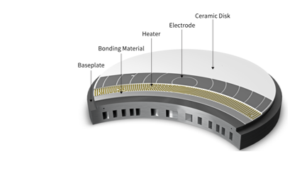
As semiconductor technology continues to evolve toward smaller nodes, higher integration density, and more complex manufacturing processes, the demand for advanced materials inside semiconductor equipment has increased dramatically. Modern semiconductor fabrication environments require materials capable of withstanding extreme temperatures, corrosive plasma exposure, ultra-clean vacuum conditions, and high mechanical stress while maintaining dimensional stability and contamination control. Among the many material solutions available today, advanced ceramics have become indispensable in semiconductor manufacturing equipment due to their exceptional combination of mechanical, thermal, electrical, and chemical properties. From wafer handling systems and etching chambers to deposition equipment and thermal processing furnaces, advanced ceramic components are widely used throughout the semiconductor production chain. Why […]
半導体製造における先進セラミック材料:高純度、高耐熱性、超硬度性能 続きを読む »