Over the past few years, most discussions about the semiconductor industry have focused on chip design, advanced process nodes and fab expansion.
But in 2026, another trend is becoming increasingly clear:
The AI boom is moving upstream into semiconductor materials.
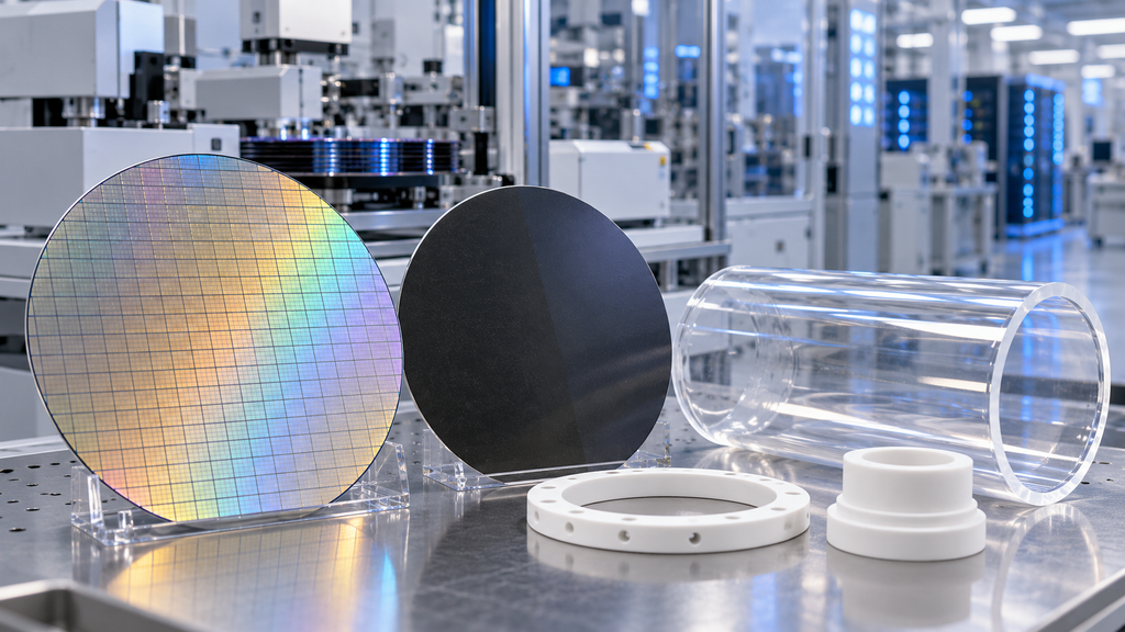
Silicon wafers, silicon carbide, high-purity quartz, advanced ceramics, carrier wafers and materials used in advanced packaging are becoming more important than ever.
The competition is also changing.
It is no longer enough for a supplier to simply prove that a material can be manufactured.
The real questions are now:
- Can defects be controlled?
- Can dimensions remain stable?
- Can purity meet advanced process requirements?
- Can the same quality be maintained from batch to batch?
- Can the supplier scale production without losing consistency?
For semiconductor materials, the next stage of competition will be increasingly defined by quality, stability and manufacturability.
1. AI Is Driving Another Wave of 300mm Fab Expansion
The rapid growth of AI servers, GPUs, HBM and high-performance computing is continuing to support investment in advanced logic and memory manufacturing.
This matters because AI demand does not stop at the chip-design level.
When fabs expand production, they also need more:
- 300mm silicon wafers
- Quartz furnace tubes
- Quartz wafer boats
- Quartz rings
- Ceramic components
- Wafer-handling parts
- Precision structural parts
- Process consumables
In other words, AI is pushing demand across the entire semiconductor manufacturing chain.
For materials suppliers, this is an important shift.
The real opportunity is not simply that more chips are being produced.
It is that advanced manufacturing requires higher-purity, tighter-tolerance and more stable materials.
2. 300mm Silicon Wafers Are Becoming Even More Strategic
The 300mm wafer remains the dominant platform for advanced logic and memory production.
As more AI chips, HBM and advanced memory products are manufactured on 300mm lines, demand for high-quality silicon wafers continues to rise.
But the key issue is no longer just wafer diameter.
For advanced semiconductor manufacturing, buyers increasingly focus on parameters such as:
- TTV
- Bow
- Warp
- Surface roughness
- Particle level
- Crystal defects
- Edge quality
- Batch-to-batch consistency
This is important because moving from smaller wafers to 300mm is not simply a matter of producing a larger disc.
A larger wafer makes dimensional control more difficult.
Even small variations can have a greater impact on downstream lithography, deposition, bonding and wafer handling.
Therefore, the real challenge in the 300mm era is not just scale.
It is stable quality at scale.
3. HBM Is Expanding the Opportunity Beyond Front-End Manufacturing
Another major effect of AI is the rapid development of advanced packaging.
HBM is a good example.
HBM is not simply a group of DRAM chips stacked together.
Its manufacturing involves technologies such as:
- Wafer thinning
- TSV
- Wafer stacking
- Bonding
- Temporary bonding
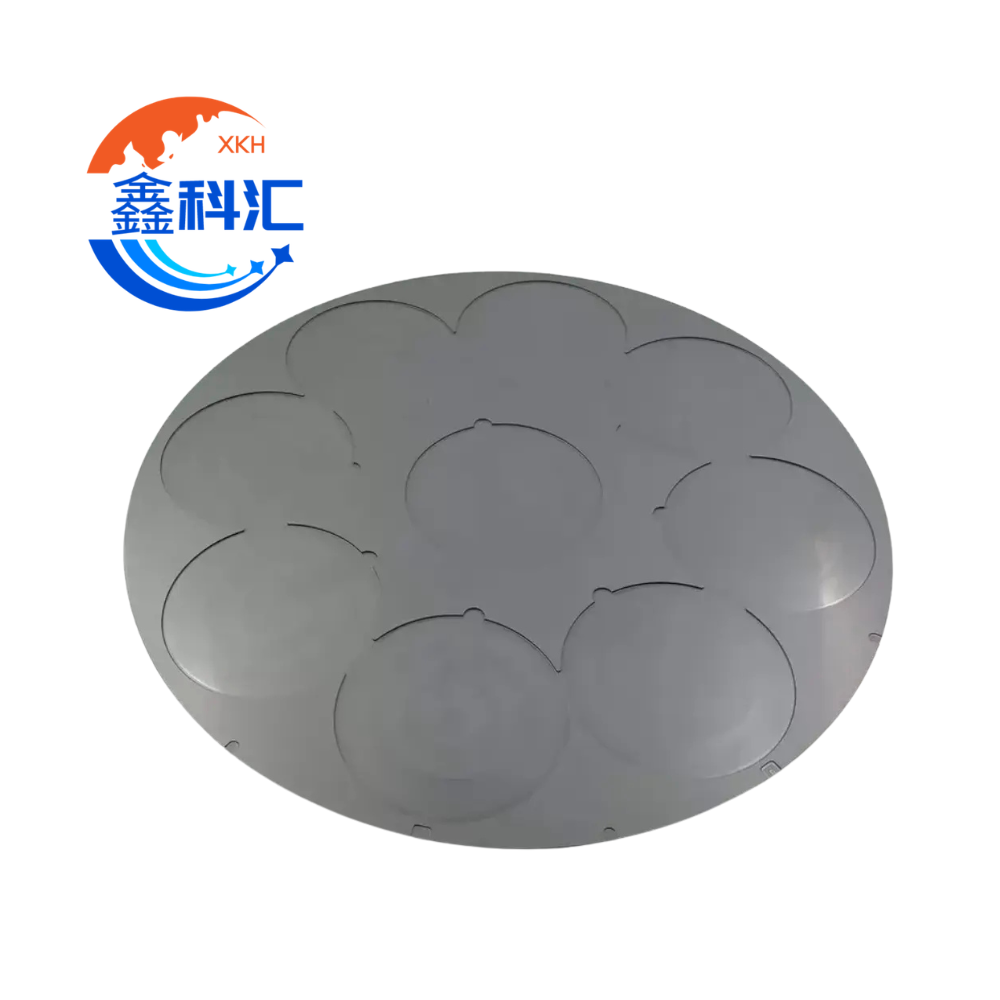
- Carrier wafers
- Advanced thermal management
- 2.5D and 3D packaging
As wafers become thinner, control of warpage, TTV, flatness and thermal expansion becomes increasingly important.
This creates new opportunities for materials including:
- Glass carrier wafers
- Fused quartz carriers
- Ceramic components
- Temporary bonding materials
- High-precision substrates
- Advanced thermal materials
The semiconductor materials market is therefore expanding from traditional wafer fabrication into advanced packaging.
This is one of the most important structural changes in the industry.
4. SiC Is Moving From Capacity Expansion to Quality Competition
A few years ago, the main question in the silicon carbide industry was:
Who can expand capacity fastest?
Then the focus shifted to:
Who can move from 6-inch to 8-inch?
Now the market is entering another stage.
The next question is:
Who can produce high-quality 8-inch SiC wafers consistently?
As 200mm SiC manufacturing develops, customers are paying more attention to:
- Micropipes
- Basal plane dislocations
- Surface defects
- TTV
- Bow
- Warp
- Wafer shape
- Surface quality
- Yield consistency
This represents a major change in the market.
In the early stage of an industry, simply having the product can create a competitive advantage.
In a more mature market, that is no longer enough.
Customers begin comparing:
defect density + consistency + yield + cost
That is exactly where the SiC market is heading.
5. High-Purity Quartz Is Becoming More Important
High-purity quartz is often overlooked because it is not as visible as silicon wafers or SiC substrates.
But it is a critical material inside semiconductor equipment.
Typical quartz components include:
- Furnace tubes
- Diffusion tubes
- Oxidation tubes
- Quartz boats
- Quartz injectors
- Quartz flanges
- Quartz rings
- Process chambers
- Custom welded quartz parts
As fabs move toward more advanced processes, quartz components face increasingly strict requirements.
Important factors include:
- Trace metal contamination
- Alkali content
- Surface cleanliness
- Particle generation
- Dimensional accuracy
- High-temperature deformation
- Devitrification resistance
- Cleaning performance
This means the future of semiconductor quartz is not simply about machining more parts.
The real competition will increasingly involve:
purity + cleanliness + dimensional control + traceability + stable production
6. Semiconductor Ceramics Are Another Quiet Growth Area
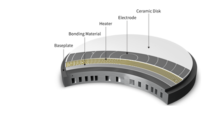
Advanced ceramics are another category that receives less public attention but plays a critical role in semiconductor equipment.
Materials such as alumina, aluminum nitride and other engineered ceramics are widely used in:
- Insulation
- Wafer handling
- Heating systems
- Vacuum equipment
- Precision motion systems
- Structural components
- Electrical isolation
- Plasma processing equipment
As semiconductor equipment becomes more sophisticated, ceramic components also require tighter specifications.
Manufacturers increasingly need to control:
- Flatness
- Surface finish
- Dimensional tolerance
- Thermal conductivity
- Electrical properties
- Purity
- Mechanical stability
For ceramic suppliers, simple machining capability is becoming less important than the ability to combine material control, precision processing and inspection.
7. Semiconductor Materials Are Entering a New Phase
If we connect the major trends together, the direction becomes clear.
AI drives demand for advanced logic and HBM.
Advanced logic and HBM support continued 300mm fab investment.
300mm expansion increases demand for wafers, quartz, ceramics and process consumables.
Advanced packaging creates new requirements for carrier wafers, bonding materials and high-precision substrates.
At the same time, SiC is moving from capacity competition toward quality and yield competition.
This means the semiconductor materials industry is entering a new phase.
The key word is not simply:
growth
It is:
upgrade
From 6-inch to 8-inch SiC.
From standard silicon wafers to tighter-specification 300mm wafers.
From conventional packaging to HBM, 2.5D and 3D integration.
From materials that are merely usable to materials that must be highly stable and highly consistent.
8. The Future Competition Will Be About Stability
As semiconductor manufacturing becomes more advanced, materials become more important, not less.
A high-value chip still depends on basic physical materials.
It still begins with:
- A wafer
- A quartz process component
- A ceramic part
- A carrier substrate
- A precision surface
If any one of these materials introduces excessive contamination, deformation or defects, the impact can spread through the entire process.
This is why future semiconductor-material suppliers will increasingly compete on five capabilities:
- Material purity
- Defect control
- Dimensional precision
- Inspection capability
- Stable mass production
The companies that can provide these consistently will have a better chance of entering high-end semiconductor supply chains.
Conclusion
AI is no longer only a competition for computing power.
It is becoming a broader industrial upgrade involving:
chips + equipment + materials + advanced manufacturing
For semiconductor materials suppliers, the biggest opportunity may not come from chasing the latest popular material.
It may come from doing the fundamentals better:
- Higher purity
- Lower defect density
- Better dimensional control
- Stronger inspection systems
- More stable production
As semiconductor manufacturing moves toward larger wafers, more advanced packaging and tighter process windows, one factor will become increasingly important:
consistency.
In the next stage of the semiconductor materials industry, the suppliers that can deliver consistent quality at scale will be the ones most likely to move up the value chain.