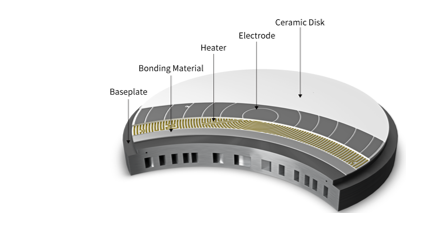
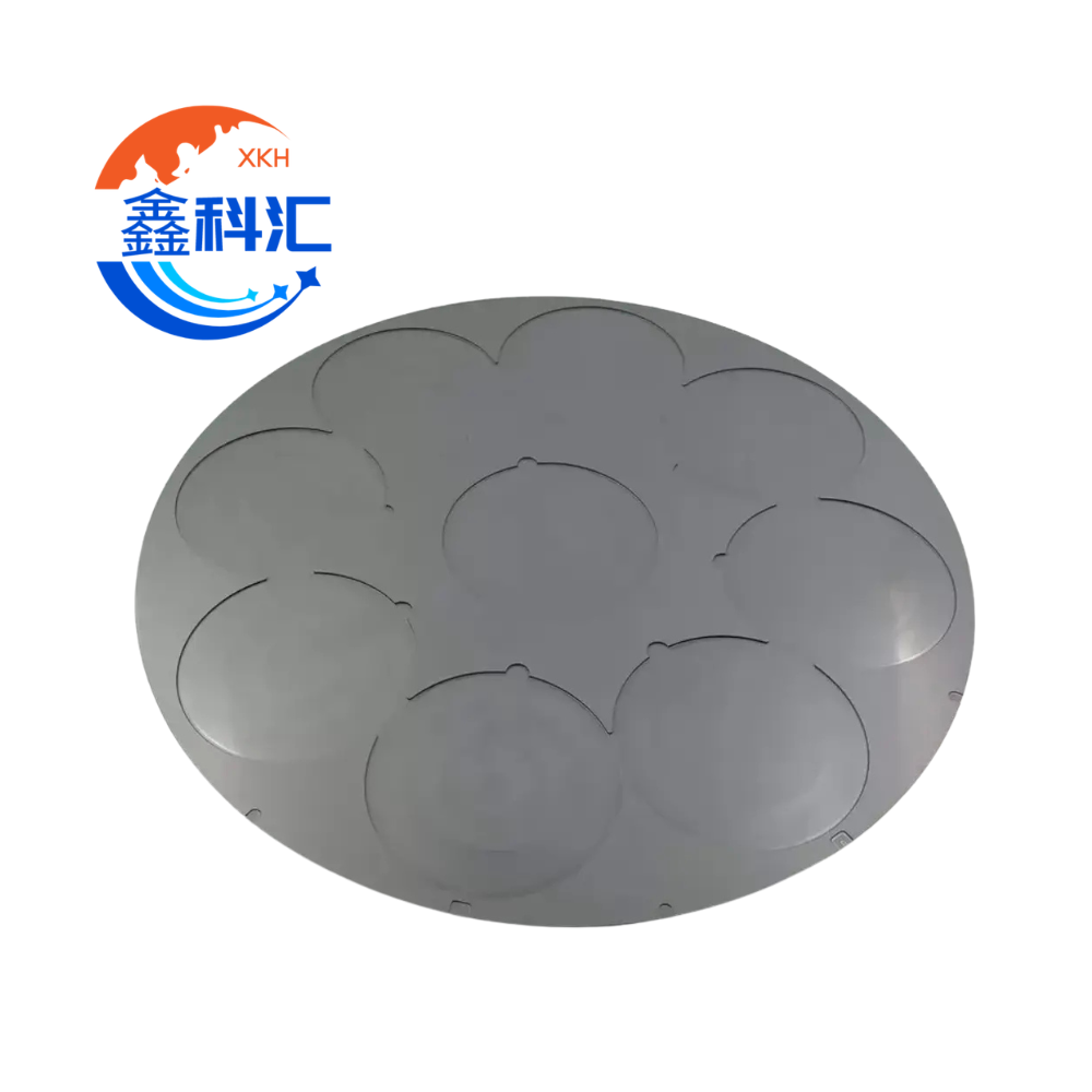
As semiconductor wafers become larger, thinner and more sensitive to mechanical stress, reliable wafer holding becomes increasingly important during inspection, grinding, dicing, metrology and other precision manufacturing processes.
A ceramic vacuum chuck provides a stable reference surface while using negative pressure to hold the wafer securely in position. Compared with conventional metal fixtures, technical ceramics offer excellent dimensional stability, wear resistance, electrical insulation and resistance to many process environments.
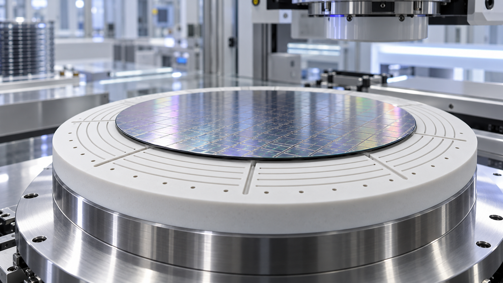
However, a high-performance wafer chuck cannot be defined simply by its material.
For semiconductor equipment, four factors are particularly important:
- Flatness and parallelism
- Porosity and pore structure
- Vacuum groove and suction-zone design
- Surface finish and wafer-contact condition
These parameters directly affect wafer deformation, positioning accuracy, vacuum uniformity, backside particle generation and ultimately process repeatability.
1. Why Ceramic Vacuum Chucks Are Used in Semiconductor Equipment
During semiconductor processing, wafers frequently need to be temporarily fixed on a precision stage.
Tyypillisiä sovelluksia ovat:
- Kiekkojen tarkastus
- Optical metrology
- Wafer grinding and thinning
- Dicing
- Wafer cleaning
- Probe and test equipment
- Alignment systems
- Wafer transfer and positioning
- Precision coating or processing equipment
The chuck must hold the wafer firmly enough to prevent lateral movement while avoiding excessive local stress.
This becomes especially important for thin wafers. If suction force is concentrated only at a few points, the wafer may locally deform toward the vacuum holes or grooves. This can influence thickness measurement, focusing accuracy, grinding uniformity or wafer geometry.
Ceramic materials such as alumina and silicon carbide are therefore widely considered for high-precision wafer support components.
Depending on the application, the chuck may use a dense ceramic structure with machined vacuum grooves or a porous ceramic surface that distributes suction through a network of microscopic pores.
2. Flatness: The Foundation of Accurate Wafer Positioning
Flatness is one of the most critical specifications for a semiconductor ceramic vacuum chuck.
When a wafer is placed on the chuck, the chuck surface effectively becomes a mechanical reference plane. Any deviation in this reference surface can influence the final position and shape of the wafer.
For example, insufficient chuck flatness may contribute to:
- Wafer bow during vacuum holding
- Non-uniform contact
- Measurement errors
- Uneven grinding or polishing
- Focus variation during optical inspection
- Positioning instability
- Local stress concentration
High-end semiconductor equipment may therefore require flatness controlled at only a few micrometers or even below the micrometer level, depending on chuck diameter, material, structure and application.
Ultra-precision ceramic chuck suppliers have demonstrated sub-micron flatness for specialized wafer-testing applications, while commercial porous ceramic chuck systems commonly specify flatness or parallelism in the several-micrometer range.
The correct tolerance should therefore be determined according to the actual equipment rather than applying one universal specification.
Important design information includes:
Wafer diameter
100 mm, 150 mm, 200 mm and 300 mm wafers create very different flatness challenges.
Chuck thickness
A thinner ceramic structure may be more susceptible to deformation during machining, mounting or vacuum loading.
Mounting method
The chuck may be mechanically fastened, bonded or integrated into another stage.
Käyttölämpötila
Temperature variation can affect both the ceramic chuck and the supporting structure.
Measurement condition
Flatness measured in a free state may differ from flatness after installation on the equipment.
For critical projects, the inspection method and datum definition should therefore be specified together with the flatness requirement.
3. Porous Ceramic Vacuum Chucks
Instead of using individual vacuum holes, a porous ceramic chuck distributes vacuum through interconnected microscopic pores across the working surface.
This creates a much more evenly distributed suction field.
Porous alumina is commonly used for this purpose because the pore structure can be engineered while maintaining good mechanical strength and wear resistance.
Typical porous ceramic vacuum chuck designs may use pore sizes ranging from a few micrometers to several tens of micrometers depending on the application. Commercial systems also commonly use porosity levels around 30–45%.
However, higher porosity does not automatically mean better performance.
The designer must balance:
- Pore diameter
- Pore distribution
- Open porosity
- Permeability
- Airflow
- Mekaaninen lujuus
- Surface integrity
- Vacuum pump capacity
Very large pores may provide high airflow but can increase local pressure differences at the wafer interface.
Very fine pores provide more distributed suction but may require different vacuum system characteristics and can be more sensitive to contamination.
For ultra-thin wafers and films, a fine and uniform pore structure is often preferred because it can reduce local deformation and suction marks.
4. Vacuum Groove Design for Dense Ceramic Chucks
Not every wafer chuck requires porous ceramic.
Dense alumina, silicon carbide and other technical ceramics can also be machined with precision vacuum grooves.
Common vacuum layouts include:
- Circular grooves
- Concentric rings
- Radial channels
- Grid patterns
- Sector designs
- Multi-zone vacuum structures
The objective is not simply to machine as many grooves as possible.
The entire airflow path must be considered.
Groove Width
Grooves must provide sufficient airflow while maintaining enough ceramic contact area to support the wafer.
If grooves are excessively wide, local unsupported areas may increase.
Groove Depth
Deeper grooves can increase internal airflow volume but may not always improve holding performance.
The appropriate depth depends on vacuum pressure, groove width, channel length and wafer geometry.
Groove Spacing
Uniform groove spacing can help distribute vacuum across the wafer.
However, groove spacing may need to change near wafer edges or in multi-zone chuck designs.
Vacuum Zones
For equipment processing different wafer sizes, independent vacuum zones can be useful.
For example, a chuck may incorporate separate suction zones for different diameters.
Only the required area is activated, helping reduce unnecessary leakage outside the wafer.
Vacuum Port Position
The location and number of vacuum connections can influence response time and pressure distribution.
For large 200 mm or 300 mm chucks, airflow paths should be designed carefully to minimize pressure differences between different areas.
5. Surface Finish Is Not Simply “The Smoother, the Better”
Surface roughness is another important specification.
At first glance, it may appear logical to polish the ceramic surface to the lowest possible Ra value.
In practice, the optimum surface depends on the chuck design and wafer-handling process.
The surface finish affects:
- Actual wafer contact area
- Friction
- Particle trapping
- Vacuum sealing behavior
- Wafer backside scratches
- Cleaning performance
An excessively rough surface may increase localized wafer contact and particle generation.
Conversely, an extremely smooth full-contact surface may not always be necessary and can increase the contact area between the wafer backside and chuck.
Some precision wafer chucks therefore use engineered contact patterns or low-contact-area designs.
For porous ceramic chucks, the finishing process becomes even more important because grinding and lapping must achieve the required flatness without improperly closing or damaging the functional pore structure.
6. Alumina vs. Silicon Carbide for Vacuum Chucks
Material selection should be based on the equipment environment rather than cost alone.
Alumiinioksidi Keraaminen
High-purity alumina is one of the most common materials used for semiconductor ceramic components.
Its advantages include:
- Korkea kovuus
- Hyvä kulutuskestävyys
- Hyvä mittapysyvyys
- Sähköinen eristys
- Hyvä kemiallinen kestävyys
- Mature precision-machining technology
- Availability in dense and porous grades
Porous alumina is especially suitable for distributed vacuum adsorption.
Piikarbidi
Silicon carbide can be selected when higher stiffness, lower thermal expansion or improved thermal performance is required.
Tyypillisiä etuja ovat muun muassa:
- Suuri ominaisjäykkyys
- Alhainen lämpölaajeneminen
- Korkea lämmönjohtavuus
- Korkea mittapysyvyys
- Erinomainen kulutuskestävyys
- Suitability for large precision structures
For high-speed stages, metrology equipment and large wafer-handling platforms, the combination of stiffness and relatively low mass can be particularly attractive.
7. Ceramic Chuck Manufacturing and Precision Machining
Producing a semiconductor-grade ceramic vacuum chuck normally requires several manufacturing stages.
Depending on the design, these may include:
- Ceramic material preparation
- Forming and sintering
- Timanttihionta
- CNC-tarkkuuskoneistus
- Vacuum groove machining
- Hole and port machining
- Lapping
- Precision surface finishing
- Puhdistus
- Mittatarkastus
- Flatness and parallelism measurement
- Vacuum performance testing
Technical ceramics are hard and brittle materials.
Machining parameters must therefore be controlled to prevent edge chipping, microcracks and subsurface damage.
Features such as small holes, thin walls, narrow vacuum channels and sharp groove intersections require particular attention.
8. Important Specifications for a Custom Ceramic Vacuum Chuck
When requesting a custom wafer chuck, equipment manufacturers should ideally provide a 2D drawing and, when possible, a 3D model.
The RFQ should include:
Materiaali
- Alumiinioksidi
- Porous alumina
- Silicon carbide
- Other technical ceramic
Overall dimensions
- Outside diameter
- Thickness
- Center-hole dimensions
Wafer size
- 4 inch
- 6 inch
- 8 inch
- 12 inch
- Custom substrate size
Flatness
Parallelism
Pinnan karheus
Porosity
Pore size
Vacuum groove dimensions
Vacuum-hole diameter
Vacuum-port configuration
Mounting-hole location
Dimensional tolerances
Käyttölämpötila
Sähkövaatimukset
Cleaning requirements
Inspection method
It is also useful to specify whether the chuck will be used for grinding, inspection, dicing, lithography, wafer transfer or another process.
The same ceramic chuck geometry may perform very differently depending on the application.
9. Custom Ceramic Vacuum Chucks for Semiconductor Equipment
As wafer dimensions increase and semiconductor equipment becomes more precise, vacuum chucks are increasingly treated as engineered precision components rather than simple workholding fixtures.
Flatness must be coordinated with wafer geometry.
Porosity must be matched to airflow and vacuum conditions.
Vacuum grooves must distribute suction without creating unsupported regions.
Surface finish must provide both precision and wafer protection.
For this reason, the best ceramic vacuum chuck design is normally developed from the complete equipment requirement.
XKH Ceramics provides custom precision ceramic components for semiconductor equipment, including alumina, porous ceramic, silicon carbide and other advanced ceramic parts.
Custom manufacturing can be developed according to customer drawings, wafer size, vacuum configuration, dimensional tolerance, surface-finish requirements and equipment interfaces.
For new vacuum chuck projects, providing the wafer diameter, ceramic material, overall dimensions, flatness requirement, vacuum structure and application allows the manufacturing feasibility to be evaluated more accurately.